![<?echo $_SERVER['SERVER_NAME'];?>](/template/twentyseventeen/skin/images/header.jpg)
Industry 4.0 has revolutionized manufacturing and changed the way factories are designed and implemented. In factory automation and process control applications, the impact of Industry 4.0 comes down to two basic concepts: the spread of decentralized systems and intelligent deterministic systems. Decentralized systems inherently require modular setup and flexibility. Efficient, low power and thermally optimized designs are key drivers for these systems. Intelligent deterministic systems are modules that detect faults early and improve reliability.
In factory automation and process control applications, digital to analog converters (DACs) are commonly found in analog outputs for programmable logic controllers (PLCs) and sensor transmitters. In both cases, the DAC can be used to transfer a voltage output or a current output.
The DAC8775 is TI's newest high-precision DAC, the most integrated in the industry by including 4-20mA drivers, voltage output and on-chip adaptive power management. In this blog post, I will provide examples of design techniques related to the DAC8775 and explore how to design current trends in the industry.
Many system controllers handle hundreds of input/output (I/O) points due to the increased number of sensors. This presents a challenge for designers to incorporate more I/O channels into a small form factor, increasing the need for thermally optimized and efficient systems. Most analog output module 4-20mA drive circuits use a high-side voltage-current conversion circuit with a gain stage. Figure 1 shows a typical architecture.
The loop established by amplifier A1 converts the DAC output voltage into a current. With negative feedback, amplifier A1 sets the voltage across RSET equal to the DAC output. This voltage drop across the RSET will set the current through the first stage IM. (I assume that IRSET is equal to the ideal case of IM). The generated current IM is further boosted by using a loop established by a combination of amplifier A2 and RMIRROR crocodile RSENSE resistor pairs. Amplifier A2 will force the voltage across RSENSE to be equal to VMIRROR. This produces a load current from the IM gain by a factor proportional to the ratio of RMIRROR and RSENSE. As shown in Figure 1, RLOAD typically represents a linear actuator load, as is the case with PLC systems. Since the current load is not provided by RMIRROR, this will directly reduce the efficiency of the system. A good design practice is to minimize this current and set it to less than 1% of the output current. For calculation purposes, assuming a high ratio between RMIRROR and RSENSE (> 1 to 100), we ignore IM.
Figure 1 : High-side voltage -to- current converter
Â
In a typical case, the VPOS voltage can vary between 12-36V. RLOAD can also vary from short resistance to 1kΩ. To illustrate this, consider our first example where VPOS is equal to 36V and RLOAD is equal to 1Ω. When the valve is set to full scale, the controller will drive 20 mA through the load. This means that the power consumed by the load is PLOAD = I2R = 0.4mW.
The total power produced is Pgenerated = = 0.72W. As can be seen from this example, the voltage-to-current conversion circuit dissipates the remaining power: 0.72W-0.4mW = 0.7196W. This is a very inefficient system and will result in an unnecessarily increased system temperature.
Consider the second example where the load impedance is high, 1kΩ. In this case, PLOAD = I2R = 0.4W. The total power produced is Pgenerated = = 0.72W. The voltage-current conversion circuit dissipates the remaining power: 0.72W-0.4W = 0.32W.
As you can imagine, adding more channels in such a small space will become unsustainable if there is a large amount of power loss, which directly increases system temperature, reduces reliability and increases failure. The example I gave shows the power loss of a single channel design. In the case where there are four channels, the power losses in the first and second examples are close to 2.8 W and 1.2 W, respectively.
Since power loss increases dramatically with the use of higher channel count modules, one possible solution is to adaptively change the VPOS supply based on the load. You can do this by adding a simple feedback network and using the buck/boost converter to provide the necessary power to the load. Such a system will be as shown in the block diagram of Figure 2.
Figure 2 : High-End Voltage -to- Current Converter with Buck / Boost Converter
Â
In this design technique, the buck/boost converter will sense the drain-source voltage of the output FET that drives the load and produce an internally proportional error current. Through complex state machine algorithms, the device will decide to reduce or boost the power supply. This technology is implemented in the four-channel DAC8775 for greater efficiency.
If you use the same value as the first example, when the load is 1Ω, the buck/boost converter will reduce the power to the DAC to get the minimum power required. In the case of the DAC8775, it will be as low as 4.5V.
As in the first example, PLOAD = I2R = 0.4mW. The total power produced is Pgenerated = VI = 0.09W. The voltage-current conversion circuit dissipates the remaining power: 0.09W-0.4mW = 89.6mW. Therefore, compared with the example 1, the power consumption is increased by 8 times.
For a 1kΩ load case, PLOAD = I2R = 0.4W. The total power generated is Pgenerated = = 0.46W because the buck/boost converter sets VPOS to 23V. The voltage-current conversion circuit dissipates the remaining power: 0.46W-0.4W = 0.06W. As a result, power consumption is increased by a factor of five compared to designs without buck/boost converter feedback.
The efficiency of the DAC8775 also leads to the need for more thermal optimization systems. Comparing the junction temperature of a chip in a four-channel design with and without an adaptive power feedback circuit shows a significant improvement in chip temperature. Figure 3 and Figure 4 show the DAC8775 measurements comparing the die temperature with and without the buck/boost converter at 1Ω and 1kΩ RLOAD. As can be seen from Figure 3, this technique can increase the junction temperature up to 36 °C.
When more and more channels are squeezed into smaller spaces, thermal optimization becomes a key performance parameter that distinguishes module functionality. In modules where heat is not optimized, system failures are common and performance is degraded due to large temperature drift. The DAC8775 addresses these two challenges due to its high level of integration and efficiency, with excellent DC and drift performance.
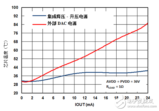
Figure 3 : RLOAD has a mold temperature of 1Ω
Â
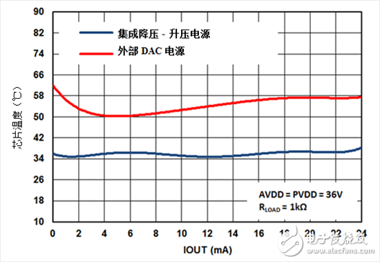
FIG 4: RLOAD mold temperature of 1KΩ
Â
If the die temperature exceeds 150°C, the DAC8775 provides an overtemperature alarm, which is one of the features of the rich intelligent diagnostics that help detect faults early. These include open load, short circuit, cyclic redundancy check (CRC), watchdog timer, and compliance voltage. In addition to fault alarms, the device allows you to select preset operations that facilitate reliable system operation. You can tell the device to do nothing, stop, or enter a pre-programmed security code.
Recommended reading:
The speed limit of the digital-to-analog converter _ digital-to-analog converter works
A text to understand the digital-to-analog converter interface isolation technology and peripheral circuits
An article to understand the important properties of an ideal digital-to-analog converter (DAC)
Glass Plate Type Liquid Level Gauge Self-closing Valve Body
Glass plate type liquid level gauge self-closing valve body,liquid level gauge self-closing valve body,self-closing valve body,liquid level gauge self-closing valve body price
Taizhou Jiabo Instrument Technology Co., Ltd. , https://www.taizhoujbcbyq.com