![<?echo $_SERVER['SERVER_NAME'];?>](/template/twentyseventeen/skin/images/header.jpg)
0 Preface
With the development of wide bandgap materials such as ZnSe and GaN and their luminescent device technology, a white LED was born in the mid-1990s. White LED has the characteristics of low driving voltage, fast switching response, no stroboscopic emission, high luminous efficiency, small size, low energy consumption, long life and strong shock resistance. It is expected to replace traditional incandescent lamps, fluorescent lamps and high-pressure gas discharge lamps. A new generation of lighting sources that are more environmentally friendly.
Since the introduction of white LEDs, great progress has been made in just a few years, from low power (mW class) to high power (W class). Currently, the highest luminous efficiency has exceeded 100 lm/W.
In China, the research and development of white LED has also received enough attention, but compared with the development of foreign countries, there is still a big gap. Among the three key technologies of white LED chip manufacturing, packaging and phosphors, packaging technology is listed as the focus of research and development in China.
1 Traditional packaging, heat dissipation and thermal matching of high-power LEDs
LED is a current-type semiconductor device that operates under constant DC drive for a long time. A large part of the energy will be converted into thermal energy, which will cause the junction temperature of the chip to rise (up to 100 °C), which leads to many problems: temperature quenching effect The light-emitting efficiency of the semiconductor light-emitting material (chip) and the phosphor is lowered, the brightness is lowered, the color temperature drift occurs during operation, the device material is deteriorated, such as yellowing of the encapsulating resin, etc.; during the switching operation of the LED, the chip is heated continuously The thermal shock, if the thermal expansion performance is not matched, will accelerate the accumulation of thermal stress and shorten its life, further reducing the reliability of LED long-term use.
To realize the practical use of LED lighting, it is necessary to develop high-power high-brightness white LEDs. In the case where the conversion efficiency is constant, to achieve high brightness, it is necessary to increase the current and the light-emitting area, which will result in a large increase in power. With the increase of power, its thermal management problem has become prominent and has become a technical bottleneck in the development of high-power LEDs.
Traditional high-power, high-brightness LED packaging methods are currently commonly used in copper or aluminum substrate packages. Although the copper or aluminum substrate can effectively improve the heat dissipation problem, the thermal expansion coefficients of copper and aluminum are 16.7 ppm/°C and 23 ppm/°C, respectively, and the LED material (5. 5 ppm/°C for GaAs and 5. 5 GaN for GaN). There is a large difference in thermal expansion coefficient between 6 ppm / °C), and the mismatch rate reaches 49.78% and 60.8%. This causes a high-power, high-brightness LED to produce a sharp drop in luminance when the switch is operating, resulting in severe degradation of product reliability. Therefore, the thermal management and packaging of high-power, high-brightness LEDs with high operating current has become a key issue in the research and development of high-power LEDs.
The packaging technology proposed in this paper not only improves the thermal expansion matching characteristics of the chip and the heat sink, but also solves the electrostatic protection problem of the high-power LED, making it longer, more economical and applicable.
2 structural design
In view of the problems existing in the traditional packaging technology of high-power LEDs, the package structure, structural materials and process technology have been improved; the LED chips on the back side are flip-chip soldered on a silicon substrate with a surge current limiting and electrostatic protection circuit, and A heat sink with a low thermal expansion coefficient is selected on the back side of the silicon substrate, and its structural schematic is shown in FIG. 1, and FIG. 2 is a schematic circuit diagram.
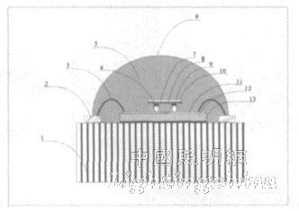
Figure 1 Schematic diagram of high power LED package structure
In Figure 1, 1: copper (aluminum) substrate heat sink heat sink; 2: lead electrode; 3: aluminum bond wire; 4: bond alloy ball; 5: high light transmission silica gel (mixed yellow phosphor); 6: spotlight Lens; 7: sapphire substrate; 8: L ED epitaxial layer; 9: indium solder layer; 10: LED metal electrode layer; 11: electrode layer of metal aluminum lead; 12: silicon base layer; 13: indium piece (solder).
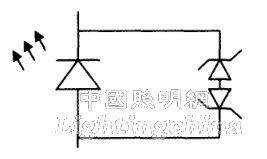
Figure 2 circuit schematic
3 material selection
3. 1 LED chip
The sapphire substrate back light emitting LED chip is used, the power is 1W, the chip area is 1 mm × 1 mm, the wavelength is 465 ~ 470 nm, the voltage is 3. 3 V, and the working current is 350 mA.
3. 2 silicon substrate
According to the electrode structure of the LED chip, the pattern size and bump size of the silicon substrate are designed, the inrush current limitation and the electrostatic protection circuit are fabricated, and the gold ball bump is formed after metallization.
3. 3 transition heat sink
In order to solve the thermal expansion mismatch bottleneck, the thermal expansion coefficient of the thermal expansion coefficient is 6. 5 ppm / K, and the thermal conductivity is 81. 6 W / (m · K).
4 Process
Using a Cu (or Al) substrate as a heat sink heat sink, and forming a lead electrode thereon;
Use a Si substrate with inrush current limiting and electrostatic protection circuit (ESD):
1) After the ESD (for the symmetrical bidirectional diode protection structure) is completed, Al is used as the electrode layer on the front side of the Si substrate, and the conventional back metallization is performed on the back surface of the Si substrate. The structure is Ti2Ni2Ag (titanium is the contact adhesion layer, and nickel is the barrier Layer, silver is the solder layer with indium);
2) At the position of the LED electrode corresponding to the Al electrode, a gold ball bump is formed by a gold ball ball welder with a diameter of 100 μm and a height of 50 μm.
3) Scribe: Cut into individual silicon-based chips with ESD protection circuits, bumps and external bonding electrodes. The device profile is shown in Figure 3.
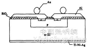
Figure 3 LED profile
Making flip-chip LED chips:
1) using a sapphire substrate, a back-emitting LED, and growing a layer of epitaxy thereon, using Ti-Ni-Ag metallization (titanium is the contact, adhesion layer, nickel is the barrier layer, silver is the reflective, conductive layer);
2) evaporating indium (thickness about 5 μm) on a Ti-Ni-Ag vacuum, and using a photolithography process to retain the indium layer on the LED electrode;
3) dicing: cutting into individual high-power LED chips;
Flip-chip soldering:
1) Use a flip-chip welder to align and bond the LED chip to the silicon substrate. When bonding, be careful that the temperature is not too high. Since indium itself is a good solder, the low temperature bonding property is good. When the temperature exceeds 156 °C, the indium layer is dissolved, and the thermal expansion buffering effect is lowered;
2) Place an indium piece with a thickness of 100 μm on a Cu (or Al) substrate (on which a layer of silver is plated); place the inverted Si-based LED chip on the indium piece and sinter at 150 °C. Soldering of flip chip and copper substrate.
3) Bonding: bonding the electrodes on the Si substrate to the electrodes on the Cu substrate (or Al substrate) with Al wires for external connection;
4) Cover the lens (there are two small holes on it), and then fill the Si glue on it (where the Si glue has high thermal conductivity and high light transmission property, and at the same time, a certain proportion of yellow phosphor is mixed in the Si glue) ;
5) curing according to the curing conditions of silica gel;
The process ends.