![<?echo $_SERVER['SERVER_NAME'];?>](/template/twentyseventeen/skin/images/header.jpg)
In this paper, we provide a new high temperature data acquisition reference design that is characterized from room temperature to 175 °C. The circuit is designed to provide a complete data acquisition circuit building block that takes analog sensor inputs, conditioned them, and characterizes them into SPI serial data streams. This design is very versatile and can be used as a single channel application or as a multi-channel simultaneous sampling application. Recognizing the importance of low power consumption, the power consumption of this ADC is linearly proportional to the sampling rate. The ADC can also be powered directly from the reference, eliminating the need for additional power rails, so there is no power conversion related inefficiency. This reference design is readily available for easy testing by designers, including full schematics, bill of materials, PCB layout and test software.
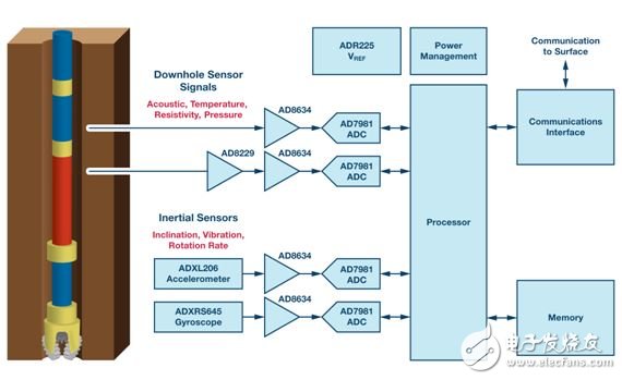
Figure 1. Downhole instrument data acquisition signal chain.
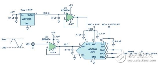
Figure 2. Simplified schematic of the data acquisition circuit.
Circuit overview
The circuit shown in Figure 1 is a 16-bit, 600 kSPS successive approximation analog-to-digital converter system with a rated temperature, characteristic test temperature, and guaranteed temperature of 175 °C. Many harsh environments are battery powered, so the signal chain is designed for low power while still maintaining high performance.
This circuit uses low power consumption (4.65 mW at 600 kSPS) and high temperature PulSAR? The ADC AD7981 is driven directly from the AD8634, a high temperature, low power op amp. The AD7981 ADC requires an external 2.4 V to 5.1 V reference. The reference for this application is the micropower 2.5 V precision reference ADR225, which is also certified for high temperature operation and has very low quiescent current (210). The maximum value is 60 μA at °C). All IC packages in this design are designed for high temperature environments, including single metal wire bonding.
Analog to digital converter
At the heart of this circuit is the AD7981, a 16-bit, low-power, single-supply ADC that uses a successive approximation architecture that supports sample rates up to 600 kSPS. As shown in Figure 1, the AD7981 uses two power supply pins: the core supply (VDD) and the digital input/output interface supply (VIO). The VIO pin can interface directly with any logic from 1.8 V to 5.0 V. The VDD and VIO pins can also be tied together to save the amount of power required by the system and they are independent of the power supply timing. Figure 3 shows the connection diagram.
The AD7981 typically consumes only 4.65 mW at 600 kSPS and automatically shuts down between conversions to save power. Therefore, the power consumption is linearly proportional to the sampling rate, making the ADC suitable for high and low sampling rates—even down to several Hz—and achieving very low power consumption and supporting battery-powered systems. In addition, oversampling techniques can be used to increase the effective resolution of low speed signals.
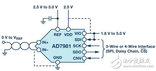
Figure 3. AD7981 application diagram.
The AD7981 has a pseudo differential analog input structure for IN+ and IN? The true differential signal between the inputs is sampled and the signals common to both inputs are suppressed. IN+ input supports unipolar, single-ended input signals from 0 V to VREF, IN? The input range is limited from GND to 100 mV. The pseudo differential input of the AD7981 simplifies ADC driver requirements and reduces power consumption. The AD7981 is available in a 10-lead MSOP package and is specified for 175°C.
ADC driver
The input to the AD7981 can be driven directly from a low impedance source; however, high source impedance can significantly degrade performance, especially total harmonic distortion (THD). Therefore, it is recommended to use an ADC driver or an operational amplifier (such as the AD8634) to drive the AD7981 input, as shown in Figure 4. At the beginning of the acquisition time, the switch is closed and the capacitive DAC injects a voltage spike (backlash) at the ADC input. The ADC driver helps stabilize this kickback and isolate it from the source.
The low-power (1 mA/amplifier) ​​dual precision op amp AD8634 is suitable for this task because its excellent DC and AC characteristics are beneficial for sensor signal conditioning and other parts of the signal chain. Although the AD8634 has a rail-to-rail output, the input requires a 300 mV margin from the positive supply rail to the negative supply rail. This necessitates a negative supply with a selected negative supply of –2.5 V. The AD8634 is available in an 8-lead SOIC package rated at 175°C and an 8-pin FLATPACK package rated at 210°C.
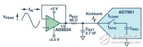
Figure 4. ADC front-end amplifier circuit.
The RC filter between the ADC driver and the AD7981 attenuates the kickback injected at the input of the AD7981 and limits the noise bandwidth entering this input. However, excessive band limiting may increase setup time and distortion. Therefore, it is important to find the optimal RC value for this filter. Its calculation is based primarily on the input frequency and throughput rate.
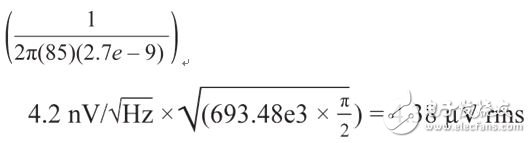
As can be seen from the AD7981 data sheet, the internal sampling capacitor CIN = 30 pF and tCONV = 900 ns, so as described, for a 10 kHz input signal, the ADC is assumed to operate at 600 kSPS and CEXT = 2.7 nF for 2.5 V. The voltage step of the reference is:
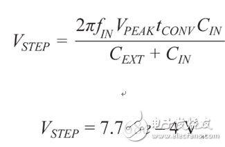
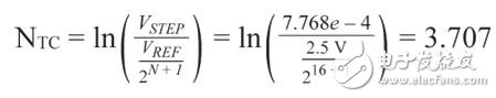
So, set up at 16th place? The number of time constants required for the LSB is:
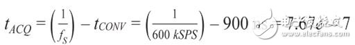
The acquisition time of the AD7981 is:
The bandwidth of the RC filter can be calculated by:
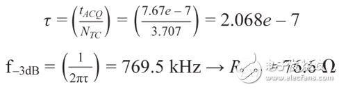
This is a theoretical value and its first-order approximation should be verified in the laboratory. Tests show that the optimal values ​​are REXT = 85 Ω and CEXT = 2.7 nF (f–3dB = 693.48 kHz), which gives excellent performance over an extended temperature range of up to 175°C.
In the reference design, the ADC driver is configured in a unity gain buffer. Increasing the ADC driver gain reduces drive bandwidth and increases setup time. In this case it may be necessary to reduce the ADC throughput rate or use a buffer as a driver after the gain stage.
Reference voltage source
The ADR225 2.5 V reference consumes only 60 μA of quiescent current at 210°C and has an ultra-low drift of 40 ppm/°C typical, making it ideal for this low-power data acquisition circuit. The device's initial accuracy is ±0.4% and operates over a wide supply range of 3.3 V to 16 V.
Like other SAR ADCs, the AD7981's reference input has a dynamic input impedance, so it must be driven with a low-impedance source. The REF pin should be effectively decoupled from GND, as shown in Figure 5. In addition to ADC driver applications, the AD8634 is also suitable as a reference buffer.
Another benefit of using a reference buffer is that the noise at the reference output can be further reduced by adding a low-pass RC filter, as shown in Figure 5. In this circuit, a 49.9 Ω resistor and a 47 μF capacitor provide a cutoff frequency of approximately 67 Hz.
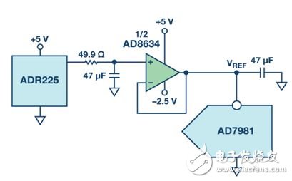
Figure 5. SAR ADC reference buffer and RC filter.
Current spikes of up to 2.5 mA may occur at the AD7981 reference input during conversion. Place a large value storage capacitor as close as possible to the reference input to provide this current and keep the noise at the reference input low. In general, low ESR – 10 μF or higher – ceramic capacitors are used, but this can be problematic for high temperature applications due to the lack of high value, high temperature ceramic capacitors available. Therefore, choosing a low ESR, 47 μF tantalum capacitor has minimal impact on circuit performance.
Digital interface
The AD7981 provides a flexible serial digital interface compatible with SPI, QSPI and other digital mainframes. The interface can be configured for simple 3-wire mode for minimum I/O count or 4-wire mode for daisy-chain readback and busy indication options. The 4-wire mode also supports independent readback timing for CNV (conversion input), allowing multiple converters to achieve simultaneous sampling.
The PMOD-compatible interface used in this reference design implements a simple 3-wire mode with SDI tied to a high-level VIO. The VIO voltage is supplied externally by the SDP-PMOD adapter board. The interposer board connects the reference design board to the ADI System Development Platform (SDP) board and connects to the PC via USB to run software and evaluate performance.
power supply
+5 V and ? of this reference design An external low noise power supply is required for the 2.5 V rail. Because the AD7981 is a low-power device, it can be powered directly from the reference buffer. This eliminates the need for additional power rails - saving power and board space. The correct configuration for powering the ADC through the reference buffer is shown in Figure 6. If the logic levels are compatible, then VIO can also be used. For reference design boards, VIO is externally powered via a PMOD-compatible interface for maximum flexibility.
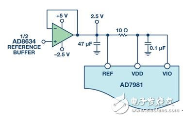
Figure 6. Powering the ADC from the reference buffer.
At 175°C, the typical total power consumption of the entire data acquisition solution can be calculated as follows:
ADR225: 30 μA &TImes; 5 V = 0.15 mW
AD8634: (1 mA & TImes; 2 amplifiers) & TImes; 7.5 V = 15 mW
AD7981: 4.65 mW @ 600 kSPS
Total power consumption = 19.8 mW
IC packaging and reliability
Devices in ADI's high temperature range undergo a special process, including design, characterization, reliability certification, and production testing. Special packaging for extreme temperatures is part of this process. The 175°C plastic package in this circuit uses a special material.
One of the main failure mechanisms of high temperature packages is the failure of the wire and pad interface, especially when gold (Au) and aluminum (Al) are mixed (as is often the case with plastic packages). High temperatures accelerate the growth of AuAl intermetallic compounds. It is these intermetallic compounds that cause soldering failures, such as fragile soldering and voids, which can occur after hundreds of hours, as shown in Figure 7.
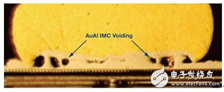
Figure 7. Gold ball bonding on an aluminum pad after 500 hours at 195 °C.
To avoid failure, Analog Devices used a pad metallization (OPM) process to create a gold pad surface for gold bond wire connections. This single metal system does not form intermetallic compounds and has been proven to be very reliable after immersion certification testing at 195 ° C for 6,000 ° C, as shown in Figure 8.

Figure 8. Gold ball bonding on the OPM pad after 6,000 hours at 195 °C.
Although ADI has proven that soldering is still reliable at 195 ° C, it is limited by the glass transition temperature of the molding material, and the maximum operating temperature of the plastic package is only 175 ° C. In addition to the 175°C product used in this circuit, the 210°C model is available in a ceramic FLATPACK package. There are also known Good Dies (KGD) available for systems that require custom packaging.
For high temperature (HT) products, Analog Devices has a comprehensive reliability certification program that includes the high temperature operating life (HTOL) that the device is biased at the highest operating temperature. The data sheet states that HT products can operate for a minimum of 1000 hours at the highest rated temperature. Comprehensive production testing is the final step in ensuring the performance of each device. Every device in the ADI High Temperature Series is tested at high temperatures to ensure performance is met.
Passive component
High temperature resistant passive components should be selected. This design uses a thin film type low TCR resistor of 175 ° C or higher. Low COG/NPO capacitance values ​​are commonly used in filters and decoupling applications with a very flat temperature coefficient. High temperature tantalum capacitors have a larger capacitance than ceramic capacitors and are commonly used for power supply filtering. The SMA connector used in this board is rated at 165 ° C, so it should be removed when tested at high temperatures for extended periods of time. Similarly, the insulation on 0.1" connector (J2 and P3) can only last for a short period of time at high temperatures and should be removed during prolonged high temperature testing. For production assembly, there are multiple suppliers. Several options are available for HT rated connectors, such as Micro-D type connectors.
PCB layout and assembly
In the PCB design of this circuit, the analog signal and digital interface are located on opposite sides of the ADC, and there is no switching signal under the ADC IC or near the analog signal path. This design minimizes noise coupled into the ADC chip and the auxiliary analog signal chain. All analog signals on the AD7981 are on the left and all digital signals are on the right. This pinout simplifies the design. The reference input REF has a dynamic input impedance and should be decoupled with very small parasitic inductance. To do this, place the reference decoupling capacitor as close as possible to the REF and GND pins and connect the reference with a low impedance wide trace. foot. The components of this board are intentionally placed on the front side to facilitate temperature testing from the back side. The complete components are shown in Figure 9.
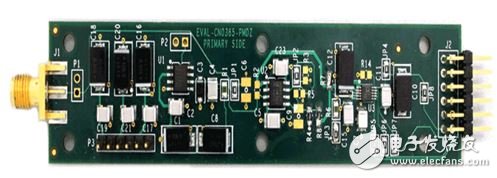
Figure 9. Reference design circuit components.
For high temperature circuits, special circuit materials and assembly techniques should be used to ensure reliability. FR4 is a commonly used material for PCB laminates, but the typical glass transition temperature for commercial FR4 is about 140 °C. Above 140 ° C, the PCB begins to crack, stratify, and put pressure on the components. An alternative material that is widely used in high temperature assembly is polyimide, which has a typical glass transition temperature greater than 240 °C. This design uses a 4-layer polyimide PCB.
The PCB surface also needs attention, especially when used with tin-containing solders, because such solders tend to form copper intermetallic compounds with copper traces. Nickel gold surface treatment is often used, in which nickel provides a barrier and gold provides a good surface for joint welding. In addition, high melting point solder should be used with a suitable margin between the melting point and the maximum operating temperature of the system. This assembly selects SAC305 lead-free solder with a melting point of 217 ° C and a 42 ° C margin relative to the maximum operating temperature of 175 ° C.
Performance expectation
With a 1 kHz input sinusoidal signal and a 5 V reference, the AD7981 has a nominal SNR of 91 dB. However, when using a lower reference voltage (such as 2.5 V, which is often the case with low power/low voltage systems), SNR performance will degrade. We can calculate the theoretical SNR based on the component specifications used in the circuit. The AD8634 amplifier data sheet shows an input voltage noise density of 4.2 nV/Hz and a current noise density of 0.6 pA/Hz. Since the AD8634 noise gain in the buffer configuration is 1 and the series input resistance can be ignored when the current noise calculation is assumed, the equivalent output noise contribution of the AD8634 is:
The total integrated noise at the ADC input after the RC filter is:
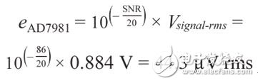
The rms noise of the AD7981 can be calculated from the typical signal-to-noise ratio (SNR, 86 dB) of the 2.5 V reference in the data sheet.
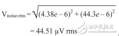
The total rms noise of the entire data acquisition system can be calculated by the square roots (RSS) of the AD8634 and AD7981 noise sources:
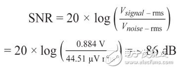
Therefore, the theoretical SNR of the data acquisition system at room temperature (25 ° C) can be approximated according to the following formula:
Test Results
The AC performance of the circuit is evaluated over a temperature range of 25 ° C to 185 ° C. Characterizing performance with a low distortion signal generator is important. This test uses the Audio Precision SYS-2522. To facilitate testing in the oven, an extension cord was used so that only the reference design circuit was exposed to high temperatures. The functional block diagram of the test setup is shown in Figure 10.
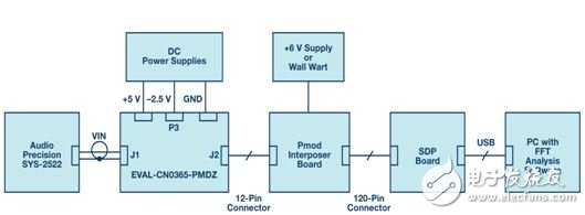
Figure 10. Feature test setup.
From the calculations in the previous settings, we expect to achieve an SNR of approximately 86 dB at room temperature. This value is comparable to the 86.2 dB SNR we measured at room temperature, as shown in the FFT summary in Figure 11.
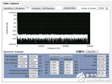
Figure 11. AC performance at 1 kHz input tone, 580 kSPS, 25 °C.
When evaluating circuit temperature performance, the SNR performance at 175 °C is only reduced to approximately 84 dB, as shown in Figure 12. Is THD still better than? 100 dB, as shown in Figure 13. The FFT summary of this circuit at 175 ° C is shown in Figure 14.
Figure 12. SNR as a function of temperature (1 kHz input tone, 580 kSPS).
Figure 13. THD changes with temperature (1 kHz input tone, 580 kSPS).
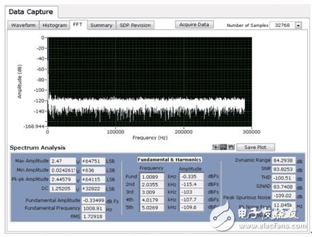
Figure 14. AC performance at 1 kHz input tone, 580 kSPS, 175 °C.
summary
In this paper, we provide a new high temperature data acquisition reference design that characterizes the temperature range from room temperature to 175 °C. The circuit is a complete low-power (20 mW) data acquisition circuit building block that takes analog sensor inputs, conditions them, and digitizes them into SPI serial data streams.
Stainless Steel Needle Valve Hydraulic Brass
Stainless steel needle valve hydraulic brass is an important part of instrument measurement pipeline system. It mainly includes stop valve and ball valve. Its function is to open or cut off pipeline passage.
Ferrule type instrument valve has the advantages of convenient installation and disassembly, tight connection, conducive to fire prevention, explosion-proof, high pressure resistance and good sealing performance. It is an advanced connection valve in power station, oil refining, chemical plant and instrument measurement pipeline. This type of valve shall be installed horizontally in the pipeline.
Stainless steel needle valve has good sealing performance and long service life. Even if the sealing surface is damaged, it only needs to replace vulnerable parts to continue to use.
During installation, the flow direction of medium shall be consistent with the arrow on the valve body.
Stainless Steel Needle Valve,Solenoid Needle Valve,Motorized Needle Valve,Pnumatic Needle Valve
Taizhou Jiabo Instrument Technology Co., Ltd. , https://www.jbcbyq.com