![<?echo $_SERVER['SERVER_NAME'];?>](/template/twentyseventeen/skin/images/header.jpg)
The switching power supply is a DC regulated power supply that utilizes a switching power device and is fabricated by power conversion technology. It has the advantages of small size, light weight, high efficiency, strong adaptability to changes in grid voltage and frequency, long output voltage retention time, and is conducive to computer information protection. It is widely used in various terminal devices led by electronic computers. Communication equipment is an indispensable power source for the rapid development of the electronic information industry. The switching power supply is also called high-efficiency energy-saving power supply. The internal circuit works in the high-frequency switching state, and the energy consumed by itself is very low. The general power efficiency can reach about 80%, which is double that of the ordinary linear regulated power supply. In the current production of power-free transformers, the switching power supply still uses the principle of pulse width modulator PWM or pulse frequency modulator PFM. According to the PWM principle, this paper introduces the design of a flyback-isolated switching regulator power supply without a power frequency transformer by using the switch BU508A.
Main technical parameters Input voltage: AC220V
Input frequency: 50Hz
Input voltage range: AC165V-265V
Output voltage: DC24V, 2A
Output power: 48W
working principle 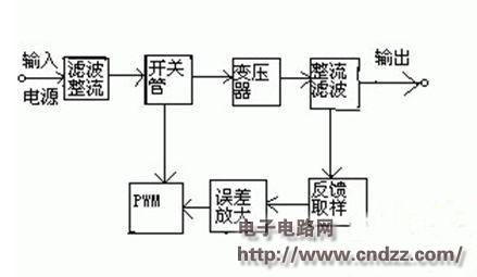
Figure 1 Working principle of the switching power supply The working principle of the switching power supply is shown in Figure 1. The input voltage is AC220v, 50Hz AC, filtered, and then rectified by the rectifier bridge to become DC, through the conduction of the switching tube in the control circuit. And the cut-off causes the low-frequency high-frequency voltage of the high-frequency transformer to be generated, and is coupled to the second measurement through the small-power high-frequency transformer, and then rectified and filtered to obtain the DC voltage output. In order to stabilize the output voltage, TL431 sampling is used, the error is optically coupled, and the on-time and off-time (ie, duty cycle) of the switching transistor are controlled by PWM, so that the output voltage remains stable.
Switching power supply design switching power supply circuit diagram shown in Figure 2. In this power conversion circuit, a single-ended flyback converter is used, and the single-ended one is because the core of the high-frequency transformer operates only in the first quadrant. According to the wiring of the secondary side switching rectifier diode of the transformer, the single-ended converter can be divided into two types: forward and flyback. The primary side main power switch tube and the secondary side rectifier tube have opposite switching states (when the switch tube is turned on, the secondary side rectifier diode is turned off), which is called a single-ended flyback type. When the primary side is applied to the high-level excitation pulse to make Q1 turn on, the DC input is input to the primary side of the high-frequency transformer. At this time, because the secondary side is up and down, the rectifier diode is turned off; when the driving pulse is low level When Q1 is cut off, the polarity of both ends of the primary side is reversed, so that the two ends of the secondary winding become upper and lower negative, the rectifier diode is forwardly turned on, and then the magnetic energy of the secondary side of the transformer is released to the load. Therefore, the single-ended flyback converter only stores energy when the primary side Q1 is turned on, and releases it to the load when it is turned off. Therefore, the high-frequency transformer functions as both a transformer and an energy storage component during the switching process. 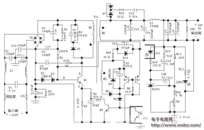
Figure 2 Switching Power Supply Circuit Diagram The EMI filter connected to the input of the AC power supply consists of common mode chokes L1, C2 and C3. The midpoints of C2 and C3 should be grounded to suppress common mode interference. C1 is used for filtering, filtering out the series mode interference, and the capacitance is large. In view of the moment when the switch BU508A is turned off, the leakage inductance of the high-frequency transformer will generate a spike voltage. C8, R3 and D1 form a clamp circuit. The function of C9 is to filter the peak voltage of the collector of the switch tube and determine the automatic restart. Frequency, C9 and R4 together compensate the control loop, while C9 and R4 also function as the primary side quick reset, which can effectively protect the switch tube from damage.
1 Switching power supply switch control part of the switching power supply whose core is the switch control part, the main working process is to control the time of the main power switch tube Q1 on and off (ie the duty ratio) through the high and low voltages of point B and point C in Fig. 2 the size of). When Q1 is turned off, point A is high level, C5 discharges to Q1, so that the potential of point B is rapidly increased, so that the base potential of the switching tube Q1 is higher than the emitter, so Q1 is saturated and turned on, and C5 is charged. At this time, the current is the sum of the current of the primary side of the transformer and the current when Q1 is turned on. Therefore, the current flowing through R5 is large, the potential at point C is increased, and the saturation conduction causes the potential at point A to drop, and Q1 is also turned off.
D2 and D3 function is to make the potential of point C not high when Q1 is turned on, otherwise the discharge time of C5 is too long, so that the turn-off time toff of Q1 is too large, and the on-time of ton remains constant, so the frequency becomes low. . If the C point rises too high when Q1 is turned on, Q1 will be turned off. At this time, D2 and D3 are forwarded, and the potential of point C is lowered, so that the discharge time of C5 is short, Vb>Vc, and toff It is also small, so the frequency can be made very high.
2 PWM adjustment section
When Q1 is turned on, the winding N2 is positive and negative, C10 absorbs the peak voltage just after discharge, preventing the diode D10 from being damaged in the forward direction, and D10 is conducting in the forward direction, so that the potential of point B rises, so that Q1 is saturated and turned on faster. At the same time, Q2 is turned on, and then Q3 is also turned on. The voltage at point B drops, and the current of the primary coil decreases to cutoff. At this time, the N2 side is positive and negative, D4 ​​and D5 are turned on, Q4 base becomes high potential, Q4 is turned on, C point potential is lowered, the cut-off time is shortened, and the TL431 feedback current causes the current flowing into the base of Q4 to be It will decrease, the potential at point C will fall slowly, and the cut-off time will become longer. When Q1 is turned on, the TL431 feedback current determines the speed at which the C point potential rises to achieve the purpose of voltage regulation. C12 is used to protect Q3, the reverse peak voltage is too high at the cutoff, and Q3 is damaged. The feedback control is to compare the sampling voltage with the reference voltage, convert it into current, and then adjust the ton and toff by current amplification to control the duty cycle to achieve the purpose of voltage regulation.
R12 is the minimum load of the output voltage, which prevents the voltage from being too high when the load is unloaded, and is used to improve the voltage regulation rate at light load. C17 can appropriately reduce the high frequency gain of the error amplifier. The reference voltage of the TL431 is compared with the output voltage Vo, and an error voltage is formed at R14, so that the diode of IC1 generates a different current. R14 is the current limiting resistor of the IC1 diode. The frequency of error amplification should be determined by R13, R16, VR, and C17. The RC absorption network consisting of C14 and R10 can eliminate high frequency self-oscillation and reduce radio frequency interference.
3 The part of the high-frequency converter is proportional to the square of the ton and the square of the DC voltage of the input primary side due to the power supplied by the primary side of the high-frequency transformer. It is inversely proportional to the number of turns of the primary winding, if not Considering the consumption of the transformer, the power of the secondary side of the transformer can be obtained by the conservation of energy, that is, the output power is independent of the number of turns of the secondary side of the transformer and the load, and is determined only by the power supplied by the primary side. Therefore, to obtain different output power, it is only by changing the power of the primary side of the high-frequency transformer. The change of ton has the greatest influence on the output power, but it is not restricted by the limitation of the magnetic flux reset condition. To change the DC voltage of the input primary side, only the parameters of the filter inductance and filter capacitor of the previous circuit can be changed, and it can also be in front. Adding a potentiometer can also change the DC voltage, and the frequency is limited by the condition of the power switch itself. Therefore, it is a good method to change the turns of the primary winding. The width of the primary winding is not too long, but it is divided into multiple layers. The access of each layer is controlled by a switch, which requires different windings. Different switches can control the power on the primary side to get different output power. However, in the toff time, the primary side magnetic flux of the high-frequency transformer should be reset, and the secondary side magnetic flux should be reset in the ton time. If the magnetic flux does not return to the starting point of the cycle start at the end of the switching duty cycle, the transformer The magnetic flux in the core will gradually increase, causing the core to saturate and damage the power switch tube. To meet the flux reset condition of the single-ended converter, it is necessary to make the time of Ton and Toff appropriate, not too long, otherwise the frequency of the switching tube becomes low, and at the same time, it is related to the number of turns of the primary side and the secondary winding of the high-frequency transformer. .
4 TL431
The TL431 is a three-terminal adjustable regulator that uses two external resistors to set any reference voltage in the range of 2.50 to 36V. The voltage temperature coefficient of the TL431 is small. Low dynamic impedance, typically 0. 2 ohms, low output noise, thermal stability specified for temperature ranges in the automotive industry, and effective output circuits with very steep turn-on characteristics, allowing these devices to be on board Regenerative, adjustable power and switching power supply applications can be a good alternative to Zener diodes.
Conclusion According to the above principle, the prototype was designed and manufactured, and the performance was stable after debugging. The characteristic of this circuit is that the duty cycle is proportional to the input voltage (the frequency is inversely proportional), and is not affected by the load, so it is easy to control in a wide range. Since the frequency of the switch tube is limited, it can reach about 50KHz-100KHz, and the power supply efficiency is slightly lower than that of the integrated switch tube. In order to improve the power efficiency of this circuit, it is better to use a switching tube with a higher frequency. The higher the frequency, the better the energy saving effect.
Tinned Copper Clad Steel,Professional Tinned Copper Clad Steel,Heat-Resistant Tinned Copper-Clad Steel,Tinned Copper Clad Steel Metal Wire
changzhou yuzisenhan electronic co.,ltd , https://www.ccs-yzsh.com