![<?echo $_SERVER['SERVER_NAME'];?>](/template/twentyseventeen/skin/images/header.jpg)
USB2.0 has a data transfer rate of 480Mbps. Universal Serial Bus (USB) has become a popular feature in mobile phones, MP3 players and other electronic products. USB makes data transfer between different electronic devices faster and more convenient, especially for products that use USB 2.0 ports.
This article refers to the address: http://
As the size of common files continues to increase, high data rates are becoming more and more important. At this level of data rate, adding any capacitance to the data line can cause signal waveform distortion, resulting in interruptions and/or failures in digital data transmission. This puts higher demands on the electrostatic discharge (ESD) protection device used on the USB 2.0 interface. The ESD protection device must remain transparent to the signal during normal data transmission, and the protected object must be protected from damage or interference when subjected to actual ESD events in the system level ESD compatibility test or application site. Today, designers face the need to find the right ESD protection solution that protects sensitive lines without the challenge of capacitors that cause signal degradation.
USB2.0 eye diagram
An eye diagram can be used to evaluate the effect of increasing capacitance on bandwidth and signal quality. The eye diagram provides digital signals with minimum and maximum voltage levels and signal jitter. The eye diagram will be able to reveal any problems with the integrity of the USB data transmission.
The eye diagram is generated by repeatedly sampling the digital signal on the vertical axis of the oscilloscope while triggering the horizontal time scan with the corresponding data rate. The resulting graphic looks like an eye, as shown in Figure 1. The larger the "eye", the higher the data integrity. A mask is usually used to define acceptable signal quality. This template consists of a matrix of hexagons and "eyes" in the middle of the "eyes". If the measured signal trace crosses the edge of the template, the signal quality is unacceptable. The USB 2.0 Signal Template Specification is provided by the USB Application Forum (USBIF, ) and can be found in Section 7.1.2.2 of the USB 2.0 Specification. An eye diagram with detailed critical points is shown in Figure 1.
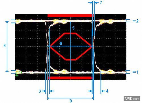
Figure 1, USB2.0 eye diagram
Eye diagram evaluation of different capacitance range protection devices. Using a USB 2.0 signal with a data rate of 480 Mbps, we measured the eye diagrams of three different protection devices with different capacitance ranges and compared them to a USB 2.0 template. We also evaluated boards without protection devices for comparison and reference. By comparing the eye diagrams of the different protection devices with the eye diagram without the protection device, the degree of signal attenuation caused by the protection device can be exhibited. It should be noted that this paper only considers the capacitance of the ESD protection diode and its influence on the USB2.0 high-speed signal. In actual design, other components on the line or the board itself may also increase the capacitance.

Figure 2. Eye diagram measured without a protective device
Figure 2 shows the test signal when there is no protection device. This represents a pure USB 2.0 high speed signal with no signal attenuation because there is no additional capacitance added to the line.
Figure 3 shows the USB 2.0 high-speed signal eye diagram with a 0.5pF capacitor ESD protection device (ON Semiconductor's ultra-low capacitance ESD device ESD9L5.0ST5G).
This eye diagram reflects no significant changes or differences in the signal. Since the capacitance value of this 0.5pF capacitor ESD device is so low, the negative effect on the integrity of the data signal is negligible. This gives designers an excellent choice of ESD protection with the highest flexibility, leaving the capacitor budget to add other components.
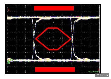
Figure 3. USB 2.0 high-speed signal eye diagram measured by adding ESD9L5.0ST5G0.5pF capacitor ESD device.
The next test used an ESD protection device with a 6.0pF capacitor (ON Semiconductor ESD9C5.0ST5G), see Figure 4. As the capacitance increases, the signal quality can be significantly reduced from the eye diagram compared to the test without increasing the capacitance. The main decline is reflected in the increase in rise time and fall time. The eye diagram shown in Figure 4 seems acceptable, but it also shows that the protection device takes up a significant portion of the capacitance budget. In most designs, other components in the design may add a large amount of capacitance, causing further degradation in signal quality. This 6.0pF capacitor ESD protection device will need to be tested in the final system design to ensure that it is still acceptable and meets compatibility requirements with the addition of additional components.

Figure 4. ESD9C5.0ST5G6pF device, where the arrow highlights the beginning of signal degradation when higher capacitive devices are used.
The final test was performed using a 65pF capacitor ESD protection device (ON Semiconductor ESD9X5.0ST5G), see Figure 5. This eye diagram shows that the signal quality is degraded severely, and the rise and fall times are shown to increase. The signal trace traverses the USB 2.0 eye pattern template, indicating that this protection device cannot be used for USB 2.0 applications.

The ESD9L5.0ST5G's ultra-low capacitance (0.5pF) provides the best semiconductor ESD protection device design choice for USB 2.0 high speed applications.
The above eye diagram study shows that the ESD9L5.0ST5G has a very low effect on the logic level and does not distort the rise and fall times. In addition to no interference with data signal transmission, the device also has an ESD rating above 8kV, providing designers with an excellent choice of ESD protection devices that not only provide the required ESD protection while maintaining signal integrity.
LiFePO4 Battery,LiFePO4 Battery Pack,Lithium Battery
LiFePO4 for Transportation Co.,Ltd , http://www.nswindenergy.com