![<?echo $_SERVER['SERVER_NAME'];?>](/template/twentyseventeen/skin/images/header.jpg)
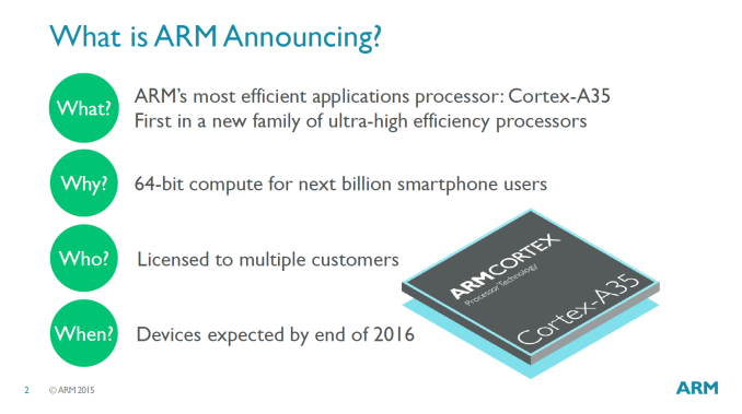
Early this morning, ARM announced its ultra-low-power processor architecture Cortex-A35 (codenamed Mercury) at its own technology conference. Vendors can redesign their architecture based on performance and power requirements and use it in different areas.
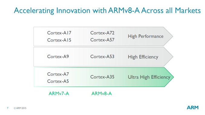
Cortex-A series is divided into three categories: high performance, low power consumption and ultra-low power consumption:
The representatives of the high-performance series are of course ARM's large core architecture Cortex A57 and A72 (also A15 and A17 which are gradually delisting);
The representative of the low-power series is the A53 high-performance ratio. According to the demand, it can work in the form of multi-core, or big.LITTLE size kernel;
In the ultra-low power series, after the A5 and A7, the A35 is now added.
Although it may seem counter-intuitive, the A35 and A53 are not a series. The A35 is the successor to the A7/A5 (ARM's product numbers have grown so fast...).
In the Exynos 5433 test, we found that the A53 as an upgraded version of the A7 still cannot maintain the power consumption level of the A7. It is more like a product that extends the A7's performance curve, which means that the A53's performance/power ratio has not improved much. But because the A53 is generally more high-frequency, it can go further on the performance side. The main energy consumption ratio of the A35 this time is in fact the A53 who blows the energy consumption ratio in the past.
However, from a strategic point of view, the most important change brought by the A35 is to make the Cortex-A series of lower and middle three-way products use the 64-bit ARMv8 architecture. After the old architecture such as A5/A7 is retired, it can complete the "64-bit" dream of the whole family. In addition, A35 and A72/A57/A53 and other cores can form big.LITTLE size SoC core structure, allowing manufacturers to come up with a combination of various sizes of nuclear products according to demand, exaggerating, and even can come up with A35+A53+ A72 SoCs with three core clusters.
Structural improvements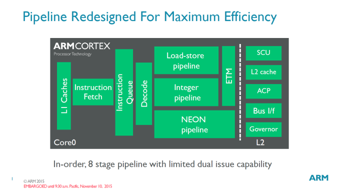
Like the A7/A53, the A35 is still a two-shot architecture that is executed sequentially. The length of the 8-stage pipeline is also no different from the previous architecture design. ARM mainly improves energy efficiency by improving individual blocks.
Key improvements are the core front-end efficiency, redesigned instruction prefetch units, and stronger branch prediction performance. In order to balance performance and power consumption, the instruction prefetch bandwidth has also been adjusted to follow the shorter queue length.
Compared to A7, A35 has a significant increase in cache speed. A35 applies a lot of A53's cache structure, a cache can be used as instruction and data cache, adding multi-threaded data prediction and write detection capabilities, according to demand can be set between 8-64KB. The L2 cache can be set between 128KB-1BM. While improving the writing efficiency and introducing the attachment optimization function to reduce the occupancy, it also improves the performance of resource sharing.
Another big improvement is the NEON/FP pipeline. In addition to improving memory performance, the new cell-wide pipeline supports double-precision multiplication calculations. The pipeline has also been improved to improve local efficiency, which is an important reason why the A35 chip area can be smaller than the A53.
In terms of power management, the A35 is also very similar to the A53, which adds state retention to the CPU and NEON pipelines (independent power supply zones) (allows the core to stay in its original state during hibernation, similar to iOS's tombstone mode). A hardware to control the CPU in and out of the reservation. Vendors rarely use this feature, temporarily confirming that this feature was introduced to the Snapdragon 810, but perhaps due to thermal issues, it also disables this feature in subsequent software updates, allowing the core to be shut down directly when the CPU is idle.
Low power / customizable / ultra-small chip area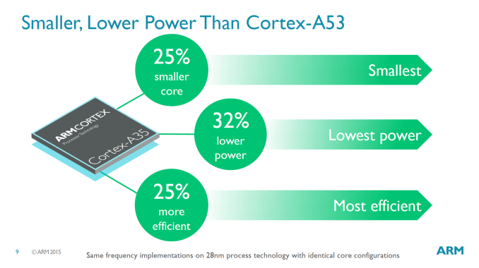
The power consumption range of the A35 is less than 125mW, which is also the normal power consumption range of the A7 and A5. In order to facilitate our brain supplement, ARM said that with the 28nm process 1GHz frequency A35 processor, its power consumption is only 90mW. Of course, just like the current A53 in different SoCs, the power consumption of the A35 core can also fluctuate greatly due to differences in the number of cores, main clocks, and process nodes (for example, using the 14/16 nm process, or pushing the main frequency to 2 GHz).
The A35 is also ARM's most customizable architecture. Vendors can choose no longer only the core number, they can choose whether to join the NEON, Crypto (encryption) and ACP (analysis) units, and even whether to join the secondary cache can choose. This makes the A35 may become the most widely used core architecture of the next generation of mobile phones, and we are also likely to see a large number of A35 processors customized for the IoT on wearable devices and embedded platforms.
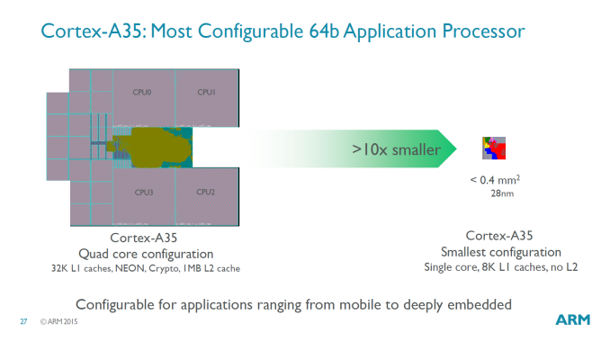
Comparing 32KB L1 cache, 1MB L2 cache, 4-core A53 with NEON/Crypto encryption module, and eliminating other parts of the single-core A35 (8KB L1 cache without L2 cache), even using the 28nm process The chip area is controlled at 0.4 square millimeters (10.4mm, which is much smaller than rice grain), which makes it very suitable for IoT chips.
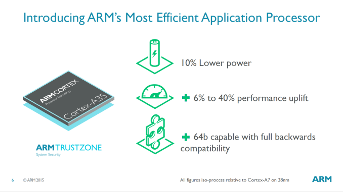
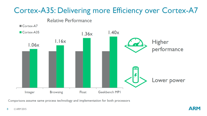
At the same core number and frequency, the A35 architecture claims 10% lower power consumption than A7 and 6-40% higher performance. In integer arithmetic (SPECint2006 test), it can be improved by 6%; in floating point arithmetic (SPECfp2000 test), the increase is even greater, up to 36%.
According to requirements, A35 can achieve A53 80-100% performance. In the browser load test, the gap between the A35 and the A53 is the largest. The A35 can only provide 80% of the performance of the A53. In the integer operation load test, the A35 can achieve the performance of A53 84-85%. For the maximum cache performance, Reflected in load testing that requires cache performance, it can have performance close to A53.
The chip area of ​​the A35 is only 75% of the A53, while the power consumption is only 68% of the A53. ARM claims that they can use it at the same time, even with SoCs that A53 has made into a large and small core architecture.
A35 can improve the performance gap with the A53 as long as the frequency is increased. Even in the worst scenario, the high-frequency A35 will eat up its own advantage in power consumption, but manufacturers can still trade in smaller chip areas, which can still save a lot of money.
If, as PPT puts it, no matter if it is composed of multi-core SoCs alone or with large cores such as the A72, it is no longer necessary to use the A53 architecture. A35 is likely to replace A53.
ARM expects that the first A35 devices will ship in late 2016. Because of its wide variety of uses and adaptations, it will undoubtedly become one of the most important core architectures in the ARM series in the coming years.
In this way, after the A35 took over the work of A5/A7, it also let the A53 collar become a...
However, as a running sub-participant, the author is more concerned about the performance of the high-performance core A72, after all, at the same time to contend with Apple's A9, Qualcomm's Kryo and Samsung's meerkats, accidentally had to take a lunch.
Via:anandtech
