![<?echo $_SERVER['SERVER_NAME'];?>](/template/twentyseventeen/skin/images/header.jpg)
1. The design of the ground plane. The low inductance ground loop is the most effective way to suppress EMC problems during PCB design. Enlarging the ground plane area and reducing the inductive reactance of the ground loop can effectively reduce radiation and crosstalk.
There are many ways to design the ground loop of a signal. The worse method is to connect the device to the ground network at will. This highly inductive ground loop design can cause unpredictable EMC problems.
The recommended method is to provide a path with the lowest impedance for signal reflow with a complete ground plane. Obviously, for a two-layer PCB, a complete ground plane is impractical. In this case, the designer can use the ground grid method, as shown in Figure 1a. In this case, the loop inductive magnitude depends on the grid spacing size.

The return of the signal is very important. A longer return path means a larger return path, which results in an antenna effect and outward radiated energy. Therefore, signal reflow should take the shortest path and connect directly to the ground plane. It is not advisable to connect all the points at a single point and connect them together to the ground plane, which not only increases the current loop size, but also increases the possibility of ground bounce. Figure 1b illustrates the recommended connection of the device to the ground plane.
Faraday cages are another way to reduce EMC problems. The Faraday cage is a suture hole that is added around the periphery of the PCB. Note that the outside of the cage is not routed.
As shown in Figure 1c, the Faraday cage effectively suppresses radiation/interference from the PCB to/from the board. It is recommended to connect all GND holes with a ground wire with a width of 200~400mils on the surface. In the signal layer, it is recommended to connect these GND holes with a ground wire with a width of 20~40mils, but it is not recommended to connect the wires into a loop.
2. Device isolation. Depending on the function, the components are grouped and placed in different locations on the PCB, such as analog signals, digital signals, power supplies, low-speed signals, and high-speed signals. Each group of signals should be in their respective assigned areas, and the signals pass between different groups (from one subsystem to the other) and filtering should be added at the boundaries.
3. Laminated design. More than two layers of design should have a complete ground plane. In a four-layer board... It should be noted that there should be a GND layer between the high speed signal layer and the high speed signal line. For a two-layer board, the complete GND plane is unrealistic and can be done in a grid point. If there is no separate power plane, it is recommended to run the GND line in parallel below the power trace to ensure stable power supply.
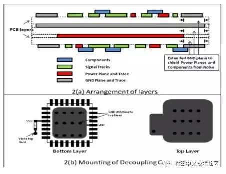
Note: The GND layer extends outward for 20h with respect to the power and device layers to shield noise. /h: spacing between power and ground plane
4. Digital circuits. When dealing with digital circuits, pay special attention to clock signals and high-speed signal lines. These signal traces should be as short as possible, and the traces should be close to the ground plane to ensure that the radiation and crosstalk are within the controllable range. For these signals, be careful to reduce the use of vias, avoid routing at the edge of the PCB, or near the connector. These signals should also be kept away from the power plane as they may couple noise to the power plane.
For the processing of the oscillator, except for isolation with GND. Be careful not to parallel or walk under the oscillator, and ensure sufficient distance from the CLK signal. The oscillator is as close as possible to the chip using the clock.
Note that the reflow is always along the lowest path of the impedance. Therefore, the GND of the load return should be as close as possible to its signal path to minimize the current loop area.
The P/N lines between the differential pairs are close to each other, which can effectively perform common mode rejection.
5. Clock termination. Pay attention to the impedance matching of the clock signal line, otherwise it will cause signal reflection. If the reflected signal is not processed, these signals will be radiated. There are a variety of effective termination methods, including source termination, end termination, and AC termination.
6. Analog circuit. The analog signal should be kept away from the high-speed transition signal and isolated by GND. Low-pass filters are commonly used in applications to filter out high-frequency noise from surrounding analog signals. In addition, the analog ground and the digital ground should be separated.
7. Decoupling capacitors. Any noise on the power supply may cause the device to work abnormally. Generally, some high-frequency noise is coupled to the power supply, which can be filtered by using a decoupling capacitor. The decoupling capacitor supplies power to the high-frequency noise. Low impedance path to GND. The signal return path constitutes a ring-shaped structure of the power supply to the ground, and the decoupling capacitor is placed as close as possible to the IC pin, so that the area of ​​the return ring is minimized. Large areas of the return loop increase radiation and become a potential cause of EMC failure.
In theory, the reactance value of a capacitor gradually approaches zero as the frequency rises. However, there is no such ideal situation. Both the package and the pin increase the equivalent inductance of the capacitor. Using multiple low ESL capacitors at the same time helps to enhance the decoupling effect.
8. Cable. Many EMC problems are caused by cables acting as antennas when high-speed signals pass through the cable. Ideally, current flows into the cable from one end and out without attenuation at the other end. The reality is that the presence of parasitic capacitance and inductance can cause radiation and create EMI problems. By suppressing the induced magnetic field through the twisted pair, the coupling can be kept at a low level. When using a strip line, be careful to provide multiple GND loops (multiple GND lines). For high frequency signals, a GND shield should be provided at both ends of the cable.
9. Crosstalk. Crosstalk exists between any two traces on the PCB. The size of the crosstalk is related to mutual inductance, mutual capacitance, edge rate of the signal, and impedance of the trace. In digital systems, crosstalk caused by mutual inductance is generally greater than crosstalk caused by mutual capacitance. The mutual inductance between the signal lines can be reduced by increasing the distance between the signal lines or by reducing the distance between the signal lines and GND.
10. Shield. Shielding is not an electronic method of reducing EMC, but an institutional means. Metallic (conductor or magnetic) housings can be used to shield EMI from outside the system. Depending on the actual requirements, the shielding can be partial or integral. The shielding cavity is equivalent to a closed grounded container, which can effectively absorb and reflect radiation and reduce the size of the loop antenna. Similarly, the shield can also be an isolation between different parts, attenuating the energy radiated from one part to the other. Shielding reduces the EMI by attenuating the E and H parameters of the radiated wave!
CIXI LANGUANG PHOTOELECTRIC TECHNOLOGY CO..LTD , https://www.cxblueray.com