![<?echo $_SERVER['SERVER_NAME'];?>](/template/twentyseventeen/skin/images/header.jpg)
Random changes require new methods, new tools, and collaboration between different companies.
Extreme ultraviolet (EUV) lithography is approaching production, but random changes, also known as random effects, are resurfaced and present more challenges for this long-awaited technology.
GlobalFoundries, Intel, Samsung and TSMC hope to add EUV lithography to 7nm and 5nm production. But as before, EUV consists of several components that must be integrated before the chip maker can introduce it. Including lithography machine, light source, photoresist and mask. Recently, the industry has begun to issue alarms about quantum random effects, which can cause random changes in lithographic patterns.
Some components are ready, while others are slow to develop. In fact, for the first time, the EUV team listed photoresist and its related issues as the biggest challenge of EUV, exceeding the power supply. After years of delay, the EUV source power finally meets the requirements of high volume production (HVM).
Photoresist is a photopolymer used to make patterns, which is one of the main culprits in causing random effects. By definition, random effects describe events with random variations in photons. They are unpredictable and have no stable patterns.
In the case of EUV, photons hit the photoresist and cause a photochemical reaction. However, for EUV photoresists, new different reactions may occur during each or more reactions due to quantum delocalization. Therefore EUV is prone to random effects. In general, the industry blames the randomness mainly on photoresist, but the EUV photomask and other parts (the EUV photon mean free path is larger) may also have random variables.
The random effects are not new. In fact, this phenomenon has been plaguing the EUV team for many years. It is well known that random effects can cause variations in lithographic patterns. The industry has been working hard to solve this problem, but people either underestimate the problem, or fail to solve the problem in time, or both.
The new situation is that the industry has finally ushered in another problem. An advanced logic chip integrates one billion or more tiny vias. If a problem occurs during EUV lithography, the chip may suffer from failure or defect due to random effects (contact missing). In other words, a chip may fail due to a defect in a contact via.
This may be a wishful thinking, but chipmakers believe they can evade the potential randomness of the 7nm process node. In fact, EUV may appear at the 7nm process node. But in the case of 5nm or even 7nm process nodes, chip makers may not be able to avoid these and other problems unless there are some new breakthroughs in the industry. Harry Levinson, senior researcher and senior technical research director at GlobalFoundries, said: "Fairly, our industry is very optimistic about our direction toward EUV lithography. We are preparing to introduce the first generation into mass production, looking forward to the second Generation of EUV lithography, resistance to random effects is definitely one of the most important issues."
Regardless of the node, EUV random effects cause problems for chip manufacturers, fab tool suppliers, and IC design groups. David Abercrombie, Director of DFM Program at Siemens, said: "From a design perspective, the random effects are indeed random because you can't predict the location and number of changes. Therefore, there is no systematic way to say that a particular layout feature should be in this. The region is modified in another region. In other words, in addition to all the sensitive features avoided, turning it into a traditional design rule constraint, there is absolutely no way to compensate for the effects of random effects in the design process."
In response, the industry is taking steps to address some of the issues. These include:
• Suppliers are improving EUV photoresist.
• Applied Materials and ASML are developing a new electron beam measurement tool that promises to detect random defects. In addition, the startup FracTIlia has devised a method to aid measurement.
• Then, with these new measurement data, chipmakers request competitive fab tool suppliers to collaborate and integrate information together.
Why is EUV?Chip manufacturers need EUV because it is becoming more and more difficult to draw tiny features using today's lithography.
Initially, chip makers will extend today's 193nm immersion lithography and multiple exposures to 10nm and 7nm process nodes. These techniques are feasible, but using them to implement specific graphics becomes more difficult. Therefore, chip manufacturers initially wanted to use EUV for the via layer of the device. They will continue to use immersion lithography and multiple exposures in other parts.
According to GlobalFoundries, in order to handle contacts/vias, in today's 7nm process node, each layer requires 2 to 4 masks. However, EUV requires only one mask per layer.
The introduction of EUV depends on the maturity of the technology. Today, ASML is shipping its first production EUV lithography machine, NXE: 3400B. 13.5nm wavelength with 13nm lithography resolution.
EUV lithography machines can expose excellent patterns, but EUV sources have not produced enough power for many years. This affects the overall productivity of the system. Now, ASML is shipping a 246-watt EUV source with a productivity of 125 wafers per hour (wph). This has reached the target level of mass production of HVM.
However, the challenge is far from over. Today's 193nm lithography machine can run uninterrupted at 250wph. However, EUV's uptime is around 70% and 80%. Michael Lercel, director of product marketing at ASML, said: "We have proven that we can achieve productivity metrics. This year's focus is on ensuring availability. Our goal is to achieve more than 90% availability."
In addition, the EUV mask protective film is not yet ready. “The film is improving. Although the light transmission is still very low, we have proven that these films can be used at 245 watts. In off-line testing with some new materials, we think they can even exceed 300 watts.â€
Photon countingPhotoresist is another challenge. For many years, the industry has used chemically amplified photoresist (CAR) in 248 nm and 193 nm lithography.
In short, a lithographic light source produces photons or light particles. The photon strikes the photochemically amplified photoresist to produce photoacid. Then, the chemically amplified photoresist is subjected to a photoacid catalyzed reaction during the baking process after the exposure.
Chemically amplified photoresists that can be used in EUV have different results after undergoing a similar process. Gregory McIntyre, director of IMEC's ​​Advanced Graphics Division, said: "In the case of EUV, the situation is much more complicated and not well understood. You have to have higher energy photons, which produce high-energy electrons and quickly transition to low-energy electrons. These electrons then interact with the material being struck. There are many unknown factors, such as how many electrons are produced, how much energy is, and more importantly, what kind of chemical reaction these electrons produce."
Another explanation is that when the system exposes the photoresist to EUV light, a certain amount of photons are fed into the photoresist. Ideally, these photons will be evenly dispersed. But one point of the photoresist may absorb 10 photons, while the other point may absorb 8 photons. This undesired result is called quantum random effects (quantum fluctuations).
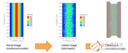
Figure 1: Random image.
In another example, it is assumed that EUV light hits the photoresist in three consecutive and separate events. In the first event, the photoresist absorbed 10 photons. The second absorption of 9 photons, the third absorption of 11 photons. This change from one event to the next is called a photon scattering noise phenomenon.
If these events are plotted on a graph curve, then the distribution of photons is sometimes undesirable. McIntyre said: "As we move toward smaller and smaller feature sizes, we will find that the Gaussian distribution begins to grow a tail and becomes asymmetrical on one side. The growth of this tail makes it more unlikely that events will occur. "(The effect of random fluctuations is greatly increased)
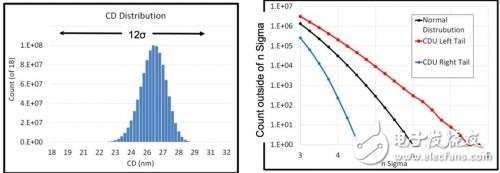
Figure 2: Gaussian distribution with tail. The chart on the right is based on 1B data points.
Random effects and scatter noise did not appear on radar screens many years ago, but the problem began to appear in 193 nm lithography. At 193 nm, the chip manufacturer used a dose of 10 mJ/cm 2 near the edge of the lithographic pattern. Chris Mack, chief technology officer of FracTIlia, explained: "If you look at the area of ​​1nm2, an average of 97 photons will pass through the area into the photoresist during the entire exposure process. However, if you look at the area of ​​10nm2, there will be an average of 9,700. a photon."
Therefore, according to Mack, when there are enough photons to generate a pattern, the photon scattering noise or random variation is only 1%. (In the case of a large number of particle statistics, quantum fluctuations can be negligible)
However, the energy of each photon of an EUV photon is 14 times higher than that of a 193 nm photon. Mack said: "This means that for the same dose, EUV has 14 times fewer photons. Therefore, in the above example, we have 97 photons exposed to 1 nm2, while EUV has only 7 photons. Certainty is one of the square roots of the number of photons. For 97 photons, this is +/- 10% uncertainty. For 7 photons, the uncertainty is +/- 40%."
What complicates the problem is that each node has a smaller feature size. When you calculate the number of photons in the lithography process, you will find that the change at this point increases exponentially.
This is not new. Over the years, Mack and others have warned: "The EUV random effect may lead to undesirable edge roughness (LER) in pattern imaging. LER is defined as the deviation of the pattern edge from the ideal shape."
LER affects the performance of the transistor. Furthermore, the LER does not shrink with feature size, so it will occupy a larger percentage in the pattern of each node.
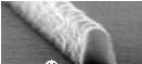
Figure 3: Line Edge Roughness (LER)
In addition to LER, the industry is now worried about other parts of the chip, especially contact vias. In operation, an EUV lithography machine produces photons that pattern the contact holes. But sometimes, this process is not perfect, resulting in random defects in the through holes. These defects appear as broken or through-hole merging, sometimes referred to as "through-hole loss and via-hole contact."
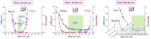
Figure 4: Random failure and shrinkage process window
These defects are catastrophic. Mack said: "The contact hole is a small dot, you have to put some photons. But if there are only a few photons, the contact hole will sometimes get 100 photons, sometimes 80, sometimes 140, the result is the size of the contact hole. Variety."
These defects may occur at the 7nm process node, but they are more likely to occur at 5nm and more advanced nodes. Mentor's Abercrombie said: "The random effects in EUV actually add random variations in the CD-controlled normal dose/focus window, as well as additional line edge roughness and lithographic dose changes. For engineers, this means more With fewer process windows, it can translate into more complex DRC design rules and fewer process reductions."
Abercrombie said: "This makes design-oriented countermeasures very ineffective, because you can't predict what will happen in any particular layout location or configuration, so you can't modify them. In fact, random effects may be average for the target. Values ​​produce positive and negative deviations and LER effects, so modifying them at a specific location may cause as much damage as there are benefits. Random effects will primarily determine which lithography/multiple exposure techniques will be used to implement the verification process. The important area required for the area and production requirements of the node."
Earphones Plug Wireless,Wireless Earphone,Earphones For Iphone,Earphone For Samsung,wireless bluetooth earphone
Shenzhen Konchang Electronic Technology Co.,Ltd , https://www.konchang.com