![<?echo $_SERVER['SERVER_NAME'];?>](/template/twentyseventeen/skin/images/header.jpg)
Electromagnetic interference (EMI) problems in design have long been a headache, especially in the automotive sector. In order to minimize electromagnetic interference, designers often reduce the noise source by reducing the loop area of ​​the high di / dt and the switching slew rate when designing the schematic and drawing the layout.
However, sometimes no matter how cautious the layout and schematic design is, it is still impossible to reduce conducted EMI to the required level. This is because the noise depends not only on the parasitic parameters of the circuit, but also on the current strength. In addition, the opening and closing of the switch produces a discontinuous current that creates a voltage ripple on the input capacitor, which increases EMI.
Therefore, it is necessary to adopt some other methods to improve the performance of conducting EMI. This article focuses on introducing input filters to filter out noise or adding shields to lock up noise.
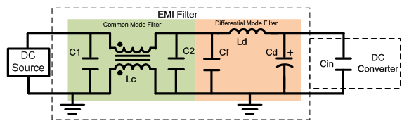
Figure 1 Schematic diagram of the EMI filter
Figure 1 is a simplified EMI filter that includes a common mode (CM) filter and a differential mode (DM) filter. Generally, the DM filter is mainly used to filter noise (DM noise) of less than 30 MHz, and the CM filter is mainly used to filter noise (CM noise) of 30 MHz to 100 MHz. But in fact, these two filters have a certain inhibitory effect on the EMI noise of the entire frequency band.
Figure 2 shows an input lead noise without a filter, including forward and negative noise, with the peak and average levels of these noises. Among them, the system under test mainly uses the chip LMR14050SSQDDARQ1 output 5V/5A, and supplies power to the subsequent chip TPS65263QRHBRQ1, and outputs 1.5V/3A, 3.3V/2A and 1.8V/2A at the same time. Both chips operate at a switching frequency of 2.2MHz. In addition, the conductive EMI standard shown in the figure is CISPR25 Class 5 (C5). For more information on this system, please refer to the application note SNVA810.
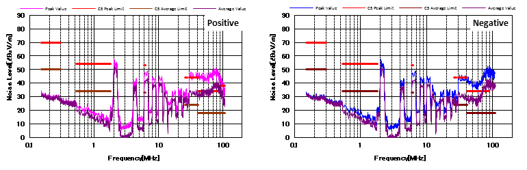
Figure 2 Noise characteristics under the C5 standard (no filter)
Figure 3 shows the EMI results after adding a DM filter. As can be seen from the figure, the DM filter attenuates the mid-band DM noise (2MHz to 30MHz) by nearly 35dBμV/m. In addition, high-band noise (30MHz to 100MHz) has also been reduced, but still exceeds the limit. This is mainly due to the limited filtering capability of the DM filter for high-band CM noise.
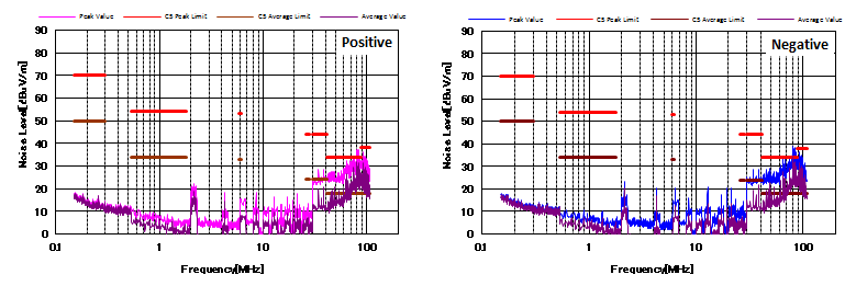
Figure 3 Noise characteristics under the C5 standard (with DM filter)
Figure 4 shows the noise characteristics after adding the CM and DM filters. Compared to Figure 3, the increase in CM filter reduces the CM noise of nearly 20 dBμV/m. And EMI performance has also passed the CISPR25 C5 standard.
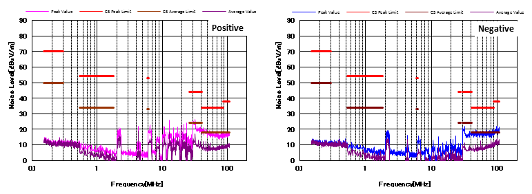
Figure 4 Noise characteristics under the C5 standard (with CM and DM filters)
Figure 5 shows the noise characteristics of the CM and DM filters with different layouts, with the filter being the same as Figure 4. However, compared with Figure 4, the noise of the entire frequency band is increased by about 10 dBμV / m, and the high frequency noise even exceeds the average value of the CISPR25 C5 standard.
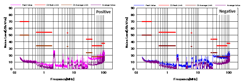
Figure 5 Noise characteristics under the C5 standard (with CM and DM filters, different layouts)
The difference in noise results between Figure 4 and Figure 5 is mainly due to differences in PCB layout, as shown in Figure 6. In the wiring of Figure 5 (on the right side of Figure 6), a large area of ​​copper (GND) surrounds the DM filter and forms some parasitic capacitance with the Vin trace. These parasitic capacitances provide an effective low impedance path for the high frequency signal bypass filter. Therefore, in order to maximize the performance of the filter, it is necessary to remove all the copper around the filter, as shown in the left side of Figure 6.

Figure 6 different PCB layout
In addition to adding filters, another effective way to optimize EMI performance is to add shields. This is because the metal shield connected to GND prevents noise from radiating outward. Figure 7 suggests a method of placing a shield. The shield covers exactly all the components on the board.
Figure 8 shows the EMI results after adding the filter and shield. As shown in the figure, the noise of the entire frequency band is almost eliminated by the shield, and the EMI performance is very good. This is mainly because the long input leads equivalent to the antenna couple a large amount of radiated noise, and the shield just isolates them. In this design, IF noise is also coupled to the input leads in this manner.
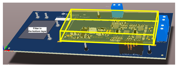
Figure 7 PCB 3D model with shield
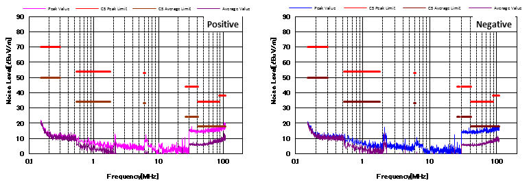
Figure 8. Noise characteristics under the C5 standard (with CM, DM filter and shield)
Figure 9 also shows the noise characteristics of the filter and shield. Unlike Figure 8, the shield in Figure 9 is a metal box that wraps the entire board and only the input leads are exposed. Despite this shield, some radiated noise can still bypass the EMI filter and couple to the power line on the PCB, which can result in worse noise characteristics than Figure 8. Interestingly, the noise characteristics of the high frequency band in Figure 4, Figure 8 and Figure 9 (same layout) are almost the same. This is because the high-band radiated noise that can be coupled to the input line is almost non-existent after the EMI filter is added.
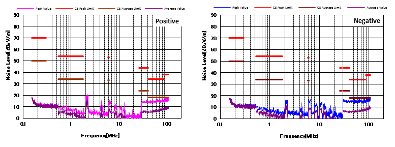
Figure 9. Noise characteristics under the C5 standard (with CM, DM filter and shielded metal box)
In summary, the addition of EMI filters or shields can effectively improve EMI performance. However, at the same time, the layout of the filter and the placement of the shield need to be carefully considered.
Spiral Rotor Flowmeter,marine helical rotor flowmeter,lzx type marine helical rotor flowmeter
Taizhou Jiabo Instrument Technology Co., Ltd. , https://www.taizhoujiabo.com