![<?echo $_SERVER['SERVER_NAME'];?>](/template/twentyseventeen/skin/images/header.jpg)
1 Introduction
Nowadays, the development trend of power management technology is that the huge market of Power over Ethernet technology is close at hand. Power ICs should be multi-disciplinary. Power conversion ICs integrate LDO and DC/DC converters, LED/LCD/OLED drivers and other power semiconductors. Device and power module. This article only discusses the dimming control technology in LED/LCD/OLED drivers. This is because LEDs have driven the lighting revolution. LCD backlights are still the main LED application, and their LEDs have been used in a variety of indoor and outdoor decorative lighting applications, and have begun to focus on general lighting applications such as flashlights, garden lights and street lights. These uses are opening up markets for LED lighting in the home and corporate lighting sector. The future of LED general lighting is the development of high-throughput LEDs with luminous efficiencies exceeding 100 lm/W, enabling LEDs to operate with AC without the need for inverters, thus driving LEDs closer to the mainstream general lighting market. Therefore, the brightness control of backlight illumination is an important technology in the LED lighting revolution, so there is an analysis of the new technical features and applications of LED illumination brightness control described below.
2, backlight illumination brightness control topology
The backlight illumination brightness control topology is a dimming method, including dimming techniques such as pulse width modulation (PWM), DC voltage control, and resistance dimming using low frequency and high frequency signals. The following only introduces DC voltage control and PWM modulation techniques.
2.1 DC voltage dimming
Figure 1 is a typical DC voltage dimming diagram using the ZETEX ZXLD1350 driver as an example.
The ZXLD1350 driver is a continuous inductive buck converter with multiple switches and an output current of 350mA with an input voltage range of 7V to 30V. Its feature is that the ZXLDl350 is equipped with a multi-function adjustment foot that adjusts the brightness of the LED in a variety of ways by controlling the current of the LED.
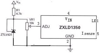
Figure 1: Schematic diagram of DC voltage dimming
   The TLV431 acts as a shunt regulator to generate an external 1.25V voltage reference. This voltage reference is applied to the VRl potential to provide a dimming voltage of 0V-1.25V. Using an external regulator will affect the accuracy of the current setting. The 1% voltage reference is used to make the LED current more accurate than the built-in voltage reference.
The adjustment pin can be overdriven with an external DC voltage (VADJ) to achieve a built-in voltage reference and adjust the output current to exceed or fall below the rated value. The rated output current at this time is:

Note that the 100% brightness setting corresponds to VADJ=VREF. If VIN reaches a maximum of 2.5V, RSENSE should be doubled. This will reduce the power by a small 1% to 2%. The input impedance of the adjustment pin is 200kV+20%. If the output impedance of the DC voltage is relatively high, it may have an effect.
2.2 New dimming technology--Application of PWM modulation technology
The wavelength at which the LED emits light is closely related to the forward current driven in the device. In order to prevent color tone changes, the dimming method must be carefully selected. The most common dimming method used in the past was to change the forward current or voltage on the device. Unfortunately, changes in current or voltage change the wavelength of the light. This effect is proportional to the wavelength, and the longer wavelengths experience the strongest change in current versus current. In many applications, this result is unacceptable. If PWM modulation is used, the LED can be properly dimmed without causing wavelength changes. The on-off operation of the LED is achieved by changing the duty cycle, where the forward current (1F) is a constant current.
2.2.1 Low frequency high frequency dimming application
(1) Low frequency dimming. Since the LED has a stable instantaneous driving current, it is suitable for low-frequency withering. The color temperature of the LED remains the same at all brightness levels. Another advantage of low frequency dimming is that the brightness can be reduced to 1%. Therefore the dimming range is 100:1. The frequency selection is to avoid visible flicker, and the PWM signal must be greater than 100 Hz. If the selected frequency is too high, the built-in low-pass filter will begin to combine the PWM signals and produce a nonlinear response. Simultaneous adjustment of the soft start function of the needle will cause a delay in the rise or fall of the PWM signal. This will give the LED current a non-linear characteristic that is more pronounced as the frequency increases.
A schematic diagram of pulse width modulation of common low frequency and high frequency signals is shown in FIG. 2 . This figure is a schematic diagram of pulse width modulation using the ZETEX ZXLD1350 driver as an example.
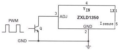
Figure 2: Schematic diagram of pulse width modulation using the ZXLD1350 driver as an example
The upper limit of the low frequency is recommended to be 1 kHz. The effects of noise that may be audible to the inductor also need to be considered. This may occur with some loosely wound inductors, which will be more pronounced than 100 Hz at a PWM frequency of 1 kHz.
(2) High frequency dimming
If the system requires low radiation and input/output harmonics, high frequency dimming is suitable. But the dimming range will drop to 5:l. The ZXLDl350 features a built-in low-pass filter that integrates high-frequency PWM signals for DC dimming control. If the PWM frequency is above 10 kHz and the duty cycle is greater than the specified minimum, the device will remain active and the output will remain unchanged.
(3) Input buffer transistor
For PWM dimming, the input bipolar transistor Q should use an open collector output (as shown in Figure 2). To ensure that the input shutdown threshold of 200mV is reached. PWM control can also be performed directly without using a buffer transistor, but care must be taken. This operation will overload the built-in 1.25V voltage reference. If 100% PWM (DC) uses a 2.5V input voltage, the output current into the LED will reach twice the normal current. And may damage the ZXLDl350. Overdriving with a 5V logic signal will most likely damage the unit beyond the rated voltage of the adjustment pin.
(4) Soft start and decoupling capacitors
Any additional capacitors on the adjustment pin will affect the PWM signal rise and fall. Since the rise time will increase by about 0.5ms/nF, this needs to be considered. Compare it with 100Hz PWM, turn on time Ton at 50% duty cycle, and off time Toff at 5ms, and turn on time Ton at 0.1% at 1% duty cycle. Adjusting the lnF on the pin will result in a rise time of 0.5ms, which will cause errors and limitations when dimming at low duty cycles.