![<?echo $_SERVER['SERVER_NAME'];?>](/template/twentyseventeen/skin/images/header.jpg)
The characteristics exhibited by the FPGA in the system are determined by the semiconductor process fabricated by the chip, and of course the relationship between them is complicated. In the past, every aspect of the process was improved at each node, and the best process choice for each new device was the latest in the smallest process. Now, the situation is no longer the case.
Instead, today's programmable logic vendors must research a variety of process choices to meet the needs of FPGA-based designs. This article describes three types of process characteristics, their relationship to the internal structure of modern FPGAs, and the impact of FPGAs on systems that use these processes. It will introduce a revolutionary revolution around the application of transistor acceleration called FinFET. How Altera uses the unique FinFET process, especially Intel's 14nm tri-gate process to further increase FPGA density, performance and efficiency, which is the development of planar FET technology. It is impossible to achieve at all.
Process characteristics
For IC designers, there are three types of process-dependent features that together represent the process. They are feature layer spacing, transistor behavior and usability.
The layer spacing is the minimum separation between similar characteristics of the finished IC, helps determine die size and capacity, and indirectly determines circuit speed and power consumption. Each feature layer of the die—transistors, local interconnects, contacts, and continuous upper metal layers—has its own layer spacing. The process engineer selects the spacing of these different layers based on lithography limits and other process constraints, costs, and how the process designer thinks the customer will use the process. These layer spacing interactions determine the actual density of transistors in a particular type of circuit.
Let's start from the bottom. How many transistors are packaged in a circuit depends roughly on two issues: how close the transistors can be, and how much spacing between the interconnects to meet their connection requirements. Both impose limitations, depending on the circuit design and layout. Of course, how close the transistor can be packaged depends on its size and shape.
From the local interconnection, the contact layer up, and the stack of metal layers above (Fig. 1), the layer distance will increase sharply. In general, the local interconnect and the underlying metal layer connect the nearby transistors, which determines the density of carefully packaged structures such as standard cells or SRAM. The upper metal layer is connected to the circuit, and finally the functional modules are connected to realize bus connection, power distribution and clock connection. The number and spacing of the upper layers is also very important for chip designers because they determine the bandwidth and power consumption of the connections between different parts of the chip.
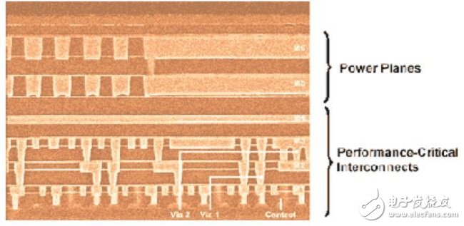
Figure 1. The higher the stack, the greater the metal layer spacing, as shown by this traditional Altera CPLD.
Transistor characteristics
In the simplest case, digital designers care only about three aspects of their transistors: how big they are, how fast transistor switches can be, and how much power they consume. Over the years, these three aspects have developed very well: the transistor size of each new process node is decreasing, the switch is faster, and the power consumption is lower.
But in recent generations, as transistor size has decreased, power consumption has been split into two distinct parts: dynamic power due to switching activity, and leakage power consumed by currents that the transistor cannot turn off. Speed ​​and dynamic power consumption have always been correlated. At each new process node, the speed is gradually increasing, the switching power consumption is slowly decreasing, and the static power consumption is increasing at each new node. Now, if you want the transistor to switch very quickly, it will leak. If you want to reduce the leakage current, the speed of the transistor will be slower. Correspondingly, at the chip level, some 28nm SoCs, half of the power consumption is static leakage power.
Process and circuit designers have countered this. Process engineers provide chip designers with a wide range of transistors with different speeds and leakage currents. Circuit designers carefully selected transistors, taking into account their turn-off clock capabilities and supply voltages to manage power efficiently. These innovations enable designers to develop cell-based digital blocks with better peak performance and lower leakage.
However, the problem with planar FETs is getting worse. In the later generations, it is increasingly difficult to further reduce the operating voltage of the planar FET. Today, many process engineers agree that it is no longer possible to reduce the latency power dissipation of planar FETs after the 20nm node: circuit designers can consider speed and power consumption around this metric. Although the best efforts have been made to extend the life cycle of traditional planar FETs, it is gradually fading out.
Today, many process designers believe that the future belongs to a new class of transistors: FinFET, which Intel calls their devices tri-gate transistors. In fact, the transistor is erected on its side. On the other three exposed side package gates, the gate of the FinFET is better able to control the current through the channel, at a fixed speed compared to a planar FET of the same size. Significantly reduced leakage (technically, lower threshold voltage). Lower leakage allows designers to achieve the required operating frequency at lower voltages while reducing dynamic and leakage power, or operating at higher speeds at a certain total power level.
Moreover, since the transistor is erected on its side, the channel width that affects the drive current does not directly limit the distance that the transistors are packaged with each other. Therefore, FinFET arrays are much denser than planar FET arrays that use the same channel width. Moreover, due to the size of the device, the FinFET is in principle more consistent than the smallest planar FET. Process engineers explain that planar devices have theoretically become so small that the number of dopant atoms in the channel can be counted. For whatever reason, some atomic errors in the production process are difficult to control, which results in a large difference in transistor threshold voltage and, therefore, electrical performance. FinFETs are much less sensitive to such changes.
FinFETs show in several ways that there are no more and more problems with planar FETs. FinFETs can be packaged closer together. They have lower, more consistent threshold voltages without unacceptable leakage currents. The lower threshold voltage support works at lower supply voltages, significantly reduces power consumption, or operates at normal voltages, but greatly increases speed.
FDA-APPROVED BLACK BARBECUE GRILL MAT
Yaxing's barbecue grill mats are made from 100% PFOA-Free materials and premium PTFE-Fiberglass coating, no PFOA, silicone or other dangerous chemicals! Certified as safe by the FDA approved! Make your meal healthier when cooking on your BBQ grill with our professional grade.
Yaxing's grill sheets are approved by the FDA and are safe for use on the top shelf of dishwasher.
Its non stick performance makes sure that nothing will stick to this grill mat. What's the most important thing is that Yaxing's grill sheets are durable and reusable.

BBQ Grill Mat,Non Stick Baking Liner,Cooking Grill Mat ,PTFE Grill Sheet
TAIZHOU YAXING PLASTIC INDUSTRY CO., LTD , https://www.yaxingptfe.com