![<?echo $_SERVER['SERVER_NAME'];?>](/template/twentyseventeen/skin/images/header.jpg)
This paper discusses the difference between the SRAM area and the FinEFT process in the Bionic and Galaxy S8 Exynos8895 chips of the iPhone 8 from the perspective of material analysis, and analyzes the difference between the nano-scale size and the selected materials, and further understands the 10 nm process of TSMC and Samsung.
The popularity of smart phones has greatly changed the way of life of modern people. The slogan that "the technology always comes from humanity" still applies. People's requirements for smart phones have always been better and faster. More energy-saving goals. Just like the iPhone 6 chip gate incident that took place in 2015, every consumer of Apple products can't wait to know if their mobile phone is using TSMC (16nm) or Samsung (when they get their mobile phone). SAMSUNG, 14nm) chip.
The two major companies in this battle have their own growth and decline. First, Samsung’s 14nm is 16nm ahead of TSMC’s 16nm, and the FinFET design of the two major manufacturers has similarities. In the end, TSMC defeated Samsung with a slight performance advantage, and made its 16nm process order for Apple's A10 processor (iPhone 7).
In 2017, Samsung made a comeback, and independently designed the Exynos8895 (named from the Greek words Exypnos and Prasinos, meaning intelligent and environmentally friendly) in 10nm technology process. It was installed on its own flagship Galaxy S8, claiming performance compared with the previous generation 14nm process. Increased by 27% and reduced power consumption by 40%. On the other hand, TSMC's 10nm product A11 Bionic was unveiled at the iPhone 8 conference this year. Apple vice president Phil Schiller made a short comment on the chip: "The smart phone has always been the most powerful and smartest chip" (The Most powerful and smartest chip ever in a smartphone).
There are new topics to discuss here. Are the two world-class semiconductor factories so weak in the new 10nm generation? Numerous analysis platforms have been evaluated for the two products. For example, Figure 1 is a comparison of Geekbench's well-known running evaluation website for two chips. We can see TSMC's A11 chip performance score, whether it is a single core 4216. The 10101 points of the multi-core or multi-core are better than the 1957 and 6433 points of the Samsung Exynos8895 respectively. There are also many articles or platforms to describe the differences between the specifications of the two major manufacturers.
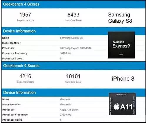
Figure 1: Performance reference provided by the Geekbench website: i8 vs. S8
This paper explores the static random access memory (SRAM) area and FinEFT of the iPhone 8 Bionic (hereinafter referred to as i8) and the Galaxy S8 Exynos8895 (hereinafter referred to as S8) from another perspective. The difference in process, supplemented by high-resolution transmission electron microscopy (TEM) image analysis technology, presents images of nanometer-scale differences, and uses the energy distribution of the micro-areas to disperse the spectral mapping analysis results (EDS mapping) to explain the two options. The difference in materials allows the reader to link the topography and composition to understand the 10nm process of the two major manufacturers.
1
SRAM size and density
We compared Intel's 14nm and 14nm+6T SRAM differences in the article "Intellect 14nm/14nm+ Evolution from a Material Analysis Perspective." The smaller the area of ​​the 6T SRAM cell, the more memory cells can be implanted in components of the same size. Figure 2 shows that at the beginning of 2017, Intel pointed out that the same size of the logic area will increase by more than 2 times when 14nm enters 10nm. Therefore, the 6T SRAM cell area is usually regarded as an important factor to measure the pros and cons of the process.
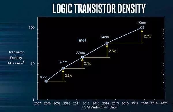
Figure 2: Intel points out the relationship between SRAM density and linewidth development
Figures 3a and 3b show the STEM image top view of the chip SRAM area of ​​the iPhone 8 (i8) and Galaxy S8 (S8), respectively. We can find that the Fin pitch in the i8 process is smaller than that of the S8, which affects the 6T SRAM. The area of ​​the unit, the area of ​​the i8 is 0.040um2, which is much smaller than the 0.049um2 of the S8. However, Figures 3c and 3d show that there is no difference in material selection between the two, so I believe that the overall performance of the i8 is superior, and the logic area is equipped with the unit. There is a relative relationship between the numbers (if the overall size of the SRAM is the same size, the number of memory units on the i8 will be 1.25 times that of the S8).
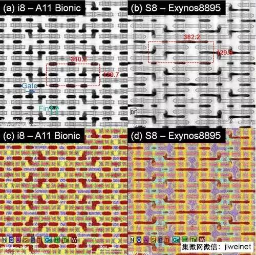
Figure 3: (a) STEM image of the i8 SRAM area; (b) STEM image of the S8 SRAM area; (c) EDS image of the i8 SRAM area; and (d) EDS image of the S8 SRAM area
2
FinFET structure and characteristics
Looking further at the difference in fin structure between the two, we can analyze the subtle differences through TEM images and EDS images. Figures 4a and 4b show the morphology of the finned ruthenium substrate in i8 and S8, including N-type (N-Fins) and P-type (P-Fins) structures.
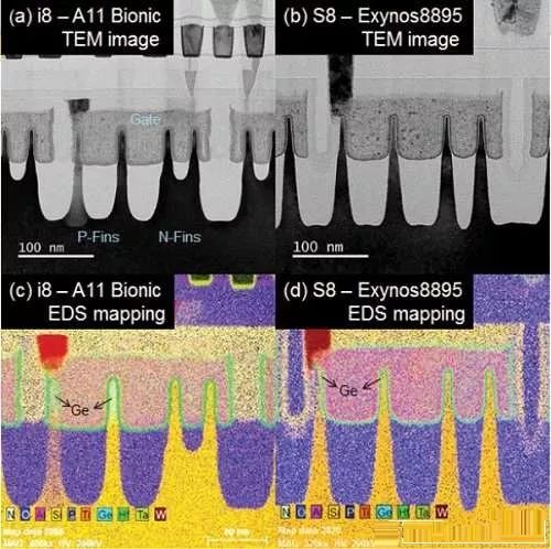
Figure 4: (a) TEM image of the i8 FinFET structure; (b) TEM image of the S8 FinFET structure; (c) EDS image of the i8 FinFET structure; and (d) EDS image of the S8 FinFET structure
There are some differences between the two designs: First, one-half of the N-Fins structure of the i8 is connected, and each fin of the S8 is very different from each other; Table 1 is unified. With some N-Fins' index sizes, we can see that the two process designs are moving in different directions. The S8 is dedicated to increasing the fin height (Fin Width) and fin width (Fin Width) in contact with the gate. Therefore, the S8 is slightly better than the i8 in both numbers. This design is completely in line with the FinFET concept of increasing the channel area. Although the i8 may be slightly smaller than the S8 in the channel area, its fin spacing is much smaller than that of the S8. Therefore, we believe that the i8 not only increases the channel area, but also reduces the size of the cell area, thus significantly increasing the number of SRAM cells.
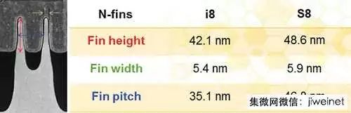
Table 1: Difference in height, width and spacing of fins: i8 vs. S8
On the other hand, the choice of materials, from the EDS images in Figures 4c and 4d, shows that the composition of the two 10nm FinFETs is similar, and there is no new material different from the previous one, but the i8 is designed on the P-Fins. There is a more unique place, we found that the obvious é”— (Ge) signal appears on the fin, and covers a third of the fin, which means that i8 directly adds é”— element to the P-Fins structure; Compared to the design of the S8, the é”— signal can also be observed at the top of the P-Fins structure, but it is very weak and only accounts for one-tenth of the total fin length.
In an article in the 2016 International Electron Device Meeting (IEDM), 'Setting the Stage for 7/5 nm', adding é”— in the fins can effectively improve the mobility of the hole. And Samsung, GLOBALFOUNDRIES, IBM have all planned to use in the 7nm process. At present, the plants have not been mass-produced or added in large quantities. The reason may be that the misalignment and defects formed after the addition of defects have not been completely overcome, but we do see that TSMC is already at 10nm. This technology is leading the way in mass production.
3
SiGe composition and strain
In the current process, the germanium (SiGe) structure grown by epitaxy utilizes the difference in lattice constant between 矽锗 and 产生 to generate strain, thereby increasing the mobility of the carrier, which makes the logic components perform at the same size. Can be greatly improved. In order to give the reader a glimpse of the overall picture of SiGe, we prepare a very thin one (according to the boundary of the high-k material at the lower edge of the gate in Figure 5 and the ghost image below it, the width of the sample we prepared is about one fin, about 5~ A 10 nm sample was used to observe the epitaxial SiGe structure above the fin.
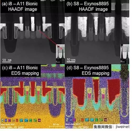
Figure 5: (a) i8 and (b) S8 parallel fin direction gate and SiGe structure; (c) i8 and (d) S8 SiGe structure at the EDS element distribution map
Figure 5 is a high-angle annular dark field (HAADF) image and its EDS mapping image of the gate and SiGe portions observed in the parallel P-Fins direction of i8 and S8. We can therefore deduce some design details: the metal contact W of the contact SiGe used in the i8 is a multi-segment design, but the S8 is a monolithic W material; on the other hand, comparing the size and area of ​​the SiGe, the SiGe of the S8 can be seen. The relative area is small, and there may be a large SiGe loss during the process. In i8, the overall structure of SiGe is better than that of S8. Finally, in the HAADF image and EDS component analysis, it can be observed that both SiGe exhibit two different concentrations of composition distribution, and the concentration of the center and the outer layer are not the same, and this design was first observed at Intel's 14nm+. It is believed that SiGe with varying concentrations should result in greater strain, allowing the mobility of the carriers to be effectively increased.
4
Metal wiring and size reduction
Finally, the SEM is used to observe the condition of the overall SRAM metal connection (Fig. 6). It can be clearly seen that the i8 is far superior to the S8 in this part, and the size of the M1 to M11 is roughly estimated. The size of the i8 is nearly 300 nm less than that of the S8. In the case where this metal connection is rapidly reduced, it is relatively a phenomenon of parasitic capacitance and signal delay (RC-delay). The influence factors of RC-delay are as follows: 20180209_10nm_NT31F1
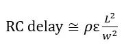
Ï= interconnect wire resistance value
ε = dielectric constant of the dielectric material surrounding the wire
L = length of metal interconnect
W= width or interconnect spacing
In the case of a rapid decrease in the wire distance W, there are two ways to reduce the RC-delay. The first is to replace the wire material with lower resistance. This is at the IEDM 2017 held in San Francisco a few days ago. Intel revealed its 10nm process node. In detail, they will replace the new material at the bottom of the two interconnect layers - cobalt, the details of this part will be further revealed in the future; the second is the use of lower dielectric constant material as low-k Floor. In the discussion of i8 and S8, no update of metal wire material was found, so we concluded that the low-k material used in i8 may be better than S8, so that it can remain efficient in the case of 300nm size optimization. can.
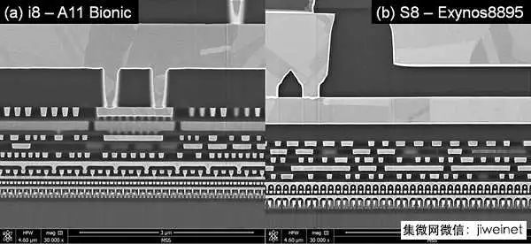
Figure 6: SEM image of a metal interconnect in a 10 nm process: (a) i8 and (b) S8
5
Conclusion
According to the FinFET of i8 and S8, from the perspective of the author, S8 moves toward the size reduction and increases the direction of the channel area, but i8 adds more ingenuity under this architectural concept and improves the overall logic area. The density, while also adding some minor differences in the process to improve performance.
Further material analysis can help the process and readers discover and understand these small differences. As the saying goes, "a little knowledge", a small SRAM area has been hidden in many small details of the design, and the final victory comes from the accumulation of each of these small details.
In order to start the process below 10nm, the process end will face more challenges in the miniaturization. At this time, the verification ability of the process, how to accurately provide the gap between several nanometers, is definitely the key to success. The powerful verification weapon brought by material analysis will become the process end and the eyes of the readers, and will be invested in each of the next battlefields.
Natural Gas Generator,Natural Gas Power Generator,Natural Gas Electrical Generator,Power Generator Natural Gas
Jiangsu Vantek Power Machinery Co., Ltd , https://www.vantekpower.com