![<?echo $_SERVER['SERVER_NAME'];?>](/template/twentyseventeen/skin/images/header.jpg)
Abstract: ApplicaTIon Note 381 contains informaTIon necessary to interface the Motorola MPC8260 processor to the DS2155 T1 / E1 / J1 Single Chip Transceiver (SCT). The applicaTIon note covers interfacing both the address and data processor bus and the communicaTIons serial bus. Interfacing the processor bus of the MPC8260 to the DS2155 is straight forward and mapping of address and data lines is discussed in detail. Depending on the application, it may be necessary to add external logic to latch the address and data pins to isolate other peripherals on the processor bus . The MPC8260 contains two serial interfaces and each has four ports for a total of eight communications serial buses. Any of the eight serial buses can be used to connect directly with the DS2155. The communication serial bus pin and clock names, and descriptions for the MPC8260 are shown in the application note tables. Example circuit diagrams are given for the processor interface as well as the communication serial interf ace. Figure 1 is an example of a master timed application where the recovered clock and transmit clock are from different sources. Figure 2 is an example of a loop timed application used in customer premises equipment where the recovered clock is used as the transmit clock. The goal of the application note is to give the designer enough information to complete a basic schematic diagram.
Interfacing the DS2155 to the Motorola MPC8260 PowerQUICC II can be accomplished many ways, depending on the intended application. The diagram in Figure 1 shows how the DS2155 is used as the master timing source in the T1 / E1 system. The oscillator is connected to the master clock (MCLK) as well as the transmit clock (TCLK). Therefore, the DS2155 sources the clock and data signal to other T1 / E1 devices. The diagram in Figure 2 shows how the DS2155 is used in a loop-timed T1 / E1 system. The oscillator is connected to the master clock (MCLK) while the recovered clock (RCLK) is connected to the transmit clock (TCLK). In this design, the DS2155 receive and transmit clocks are locked.
The local bus interface in these two diagrams is identical. Although there is a dedicated local bus on the MPC8260, the pins of this bus are shared with the PCI interface pins. Because of this, the choice was made to connect the DS2155 off of the MPC8260 60x bus with minimal interface circuitry. For the 32-bit address bus, two 74ALVC16373 16-bit latch devices are connected to isolate the peripherals from the 60x bus. On the 64-bit data bus, four 74ALVC16245 16-bit transceiver devices are connected to isolate the peripherals from the 60x bus. Depending on the complexity and number of peripherals that are connected in this fashion to the 60x, the extra inverter and the AND gate for the data bus might not be necessary. The BCTL0 line can be configured for RD / WR * or RD * / WR, which may eliminate the need for the inverter depending on the peripherals that are connected. Also, if the peripheral address space is contiguous, the AND gate could be replaced by one of the 12 chip- select lines on th e MPC8260. It is also important to note the reversing of the address and data lines of the MPC8260. The DS2155 address lines A [7–0] map to the 60x bus address lines A [24–31]. Likewise, the DS2155 data lines AD [7–0] map to the 60x bus data lines D [0–7]. In addition, if no other peripherals are connected to the 60x bus, it is possible to reduce both the number and bit size of the latch and transceiver devices since the DS2155 is only an 8- bit device.
The MPC8260 has two separate serial interface (SI1 and SI2) blocks, each of which has a time-slot assigner (TSA) that supports four time-division-multiplexed (TDM) channels. The four TDM channels for SI1 are referred to as TDMa1 , TDMb1, TDMc1, and TDMd1. All of the associated signals and physical pins for SI1 are described in Table 1. The four TDM channels for SI2 are referred to as TDMa2, TDMb2, TDMc2, and TDMd2 (Table 2). For flexibility, each TDM channel can have a separate transmit and receive clock. The source of both the transmit and receive clock can be from two different clock inputs. Table 3 contains all eight TDM channels and the two possible clock sources for the transmit and receive channel.
To simplify the circuits in Figure 1 and Figure 2, TDMa1 was chosen at the transmit and receive path for the DS2155 data. A system that incorporated up to eight DS2155s could be easily obtained by using all eight TDM channels from the two SI blocks. For more information about the operation of the TSA in the MPC8260, see the MPC8260 PowerQUICC II User's Manual. Chapter 14 of the user manual contains information about how to configure each TDM channel and how the data is stored in memory.
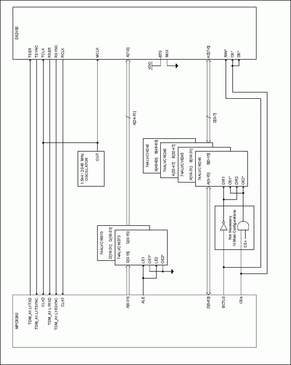
Figure 1. DS2155 Master Timing Source.
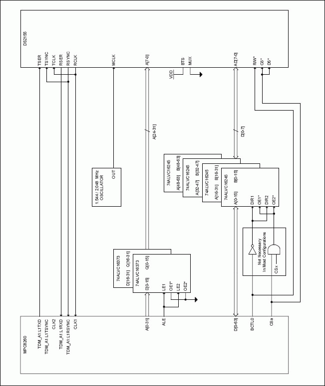
Figure 2. DS2155 Loop Timed.
Table 1. MPC8260 Serial Interface 1
Table 2. MPC8260 Serial Interface 2
Table 3. MPC8260 Serial Interface Clock Matrix
HP series High power high-voltage power supply is the first generation high-power HVPS designed by iDealTek-Electronics, adopting the standard 19-inch chassis structure to facilitate the integrated installation of high-voltage systems. The output power ranges from 5kW to 15kW (single unit), with the output voltage ranging from 1KV to 60kV.
HPS series ultra-high-power high-voltage power supplies are developed on the basis of HP series using internal high-power high voltage modules in parallel built in 19-inch standard cabinet with control, inverter, high voltage transformer split design structure, output power ranges from 50KW to 300KW with output voltage up to 300KV. The power supplies adopt a mixed cooling method of air cooling of the control part, water cooling and oil cooling of the main power unit. The internal module redundancy technology and perfect protection circuit ensure the excellent reliability of the power supply under high-voltage and high-power output.
Compared with the traditional linear high power High Voltage Power Supplies, our high-power high voltage power supplies of IGBT-based topology can achieve output power beyond that of the linear high voltage power supplies and also break through the ceiling where the output voltage cannot exceed tens of KV, besides the same electronic characteristics of high precision low ripple and high stability as the linear high-voltage power supplies, our high power high voltage power supplies are also featured for high efficiency, fast response characteristics that linear high voltage power supply can't match.
At present, the production of high power high voltage power supplies is difficult and the applications are diverse and scattered. Basically, they are mainly customized. The industries that have been aiding include mining gravel, ultra-high-power capacitor charging, electron beam melting, electron gun, ion acceleration, ion implantation and other cutting-edge industries.
Interfacing the DS2155 to the Motorola MPC8260 PowerQUICC II can be accomplished many ways, depending on the intended application. The diagram in Figure 1 shows how the DS2155 is used as the master timing source in the T1 / E1 system. The oscillator is connected to the master clock (MCLK) as well as the transmit clock (TCLK). Therefore, the DS2155 sources the clock and data signal to other T1 / E1 devices. The diagram in Figure 2 shows how the DS2155 is used in a loop-timed T1 / E1 system. The oscillator is connected to the master clock (MCLK) while the recovered clock (RCLK) is connected to the transmit clock (TCLK). In this design, the DS2155 receive and transmit clocks are locked.
The local bus interface in these two diagrams is identical. Although there is a dedicated local bus on the MPC8260, the pins of this bus are shared with the PCI interface pins. Because of this, the choice was made to connect the DS2155 off of the MPC8260 60x bus with minimal interface circuitry. For the 32-bit address bus, two 74ALVC16373 16-bit latch devices are connected to isolate the peripherals from the 60x bus. On the 64-bit data bus, four 74ALVC16245 16-bit transceiver devices are connected to isolate the peripherals from the 60x bus. Depending on the complexity and number of peripherals that are connected in this fashion to the 60x, the extra inverter and the AND gate for the data bus might not be necessary. The BCTL0 line can be configured for RD / WR * or RD * / WR, which may eliminate the need for the inverter depending on the peripherals that are connected. Also, if the peripheral address space is contiguous, the AND gate could be replaced by one of the 12 chip- select lines on th e MPC8260. It is also important to note the reversing of the address and data lines of the MPC8260. The DS2155 address lines A [7–0] map to the 60x bus address lines A [24–31]. Likewise, the DS2155 data lines AD [7–0] map to the 60x bus data lines D [0–7]. In addition, if no other peripherals are connected to the 60x bus, it is possible to reduce both the number and bit size of the latch and transceiver devices since the DS2155 is only an 8- bit device.
The MPC8260 has two separate serial interface (SI1 and SI2) blocks, each of which has a time-slot assigner (TSA) that supports four time-division-multiplexed (TDM) channels. The four TDM channels for SI1 are referred to as TDMa1 , TDMb1, TDMc1, and TDMd1. All of the associated signals and physical pins for SI1 are described in Table 1. The four TDM channels for SI2 are referred to as TDMa2, TDMb2, TDMc2, and TDMd2 (Table 2). For flexibility, each TDM channel can have a separate transmit and receive clock. The source of both the transmit and receive clock can be from two different clock inputs. Table 3 contains all eight TDM channels and the two possible clock sources for the transmit and receive channel.
To simplify the circuits in Figure 1 and Figure 2, TDMa1 was chosen at the transmit and receive path for the DS2155 data. A system that incorporated up to eight DS2155s could be easily obtained by using all eight TDM channels from the two SI blocks. For more information about the operation of the TSA in the MPC8260, see the MPC8260 PowerQUICC II User's Manual. Chapter 14 of the user manual contains information about how to configure each TDM channel and how the data is stored in memory.
Figure 1. DS2155 Master Timing Source.
Figure 2. DS2155 Loop Timed.
Table 1. MPC8260 Serial Interface 1
| SIGNAL NAME | PORT PIN | DESCRIPTION |
| TDM_A1: L1TXD [0] TDM_B1: L1TXD TDM_C1: L1TXD TDM_D1: L1TXD | PA9 PD13 PB15 / PD28 PB11 / PD25 | Transmit data output for the serial interface TDM channel. |
| TDM_A1: L1RXD [0] TDM_B1: L1RXD TDM_C1: L1RXD TDM_D1: L1RXD | PA8 PD12 PB14 / PD27 PB10 / PD24 | Receive data input for the serial interface TDM channel. |
| TDM_A1: L1TSYNC / GRANT TDM_B1: L1TSYNC / GRANT TDM_C1: L1TSYNC / GRANT TDM_D1: L1TSYNC / GRANT | PA7 PD11 PB13 / PD16 PB9 / PD4 | Transmit data sync signal for the serial interface TDM channel. |
| TDM_A1: L1RSYNC TDM_B1: L1RSYNC TDM_C1: L1RSYNC TDM_D1: L1RSYNC | PA6 PD10 PB12 / PD26 PB8 / PD23 | Receive data sync signal for the serial interface TDM channel. |
| TDM_A1: L1RQ TDM_B1: L1RQ TDM_C1: L1RQ TDM_D1: L1RQ | PB17 PB13 PC7 PC13 | D-channel request signal for the serial interface TDM channel. |
| TDM_A1: L1CLKO TDM_B1: L1CLKO TDM_C1: L1CLKO TDM_D1: L1CLKO | PB16 PB12 PC6 PC11 | Clock output from the serial interface TDM channel. |
| SI1: L1ST1 SI1: L1ST2 SI1: L1ST3 SI1: L1ST4 | PC9 PC8 PC12 PC10 | Four output strobes that can be generated by the serial interface. |
Table 2. MPC8260 Serial Interface 2
| SIGNAL NAME | PORT PIN | DESCRIPTION |
| TDM_A2: L1TXD [0] TDM_B2: L1TXD TDM_C2: L1TXD TDM_D2: L1TXD | PA9 PD13 PB15 / PD28 PB11 / PD25 | Transmit data output for the serial interface TDM channel. |
| TDM_A2: L1RXD [0] TDM_B2: L1RXD TDM_C2: L1RXD TDM_D2: L1RXD | PA8 PD12 PB14 / PD27 PB10 / PD24 | Receive data input for the serial interface TDM channel. |
| TDM_A2: L1TSYNC / GRANT TDM_B2: L1TSYNC / GRANT TDM_C2: L1TSYNC / GRANT TDM_D2: L1TSYNC / GRANT | PA7 PD11 PB13 / PD16 PB9 / PD4 | Transmit data sync signal for the serial interface TDM channel. |
| TDM_A2: L1RSYNC TDM_B2: L1RSYNC TDM_C2: L1RSYNC TDM_D2: L1RSYNC | PA6 PD10 PB12 / PD26 PB8 / PD23 | Receive data sync signal for the serial interface TDM channel. |
| TDM_A2: L1RQ TDM_B2: L1RQ TDM_C2: L1RQ TDM_D2: L1RQ | PB17 PB13 PC7 PC13 | D-channel request signal for the serial interface TDM channel. |
| TDM_A2: L1CLKO TDM_B2: L1CLKO TDM_C2: L1CLKO TDM_D2: L1CLKO | PB16 PB12 PC6 PC11 | Clock output from the serial interface TDM channel. |
| SI2: L1ST1 SI2: L1ST2 SI2: L1ST3 SI2: L1ST4 | PC9 PC8 PC12 PC10 | Four output strobes that can be generated by the serial interface. |
Table 3. MPC8260 Serial Interface Clock Matrix
| Clock | CLK pin | |||||||||||||||||||
| 1 | 2 | 3 | 4 | 5 | 6 | 7 | 8 | 9 | 10 | 11 | 12 | 13 | 14 | 15 | 16 | 17 | 18 | 19 | 20 | |
| TDMA1_Rx | V | V | ||||||||||||||||||
| TDMA1_Tx | V | V | ||||||||||||||||||
| TDMB1_Rx | V | V | ||||||||||||||||||
| TDMB1_Tx | V | V | ||||||||||||||||||
| TDMC1_Rx | V | V | ||||||||||||||||||
| TDMC1_Tx | V | V | ||||||||||||||||||
| TDMD1_Rx | V | V | ||||||||||||||||||
| TDMD1_Tx | V | V | ||||||||||||||||||
| TDMA2_Rx | V | V | ||||||||||||||||||
| TDMA2_Tx | V | V | ||||||||||||||||||
| TDMB2_Rx | V | V | ||||||||||||||||||
| TDMB2_Tx | V | V | ||||||||||||||||||
| TDMC2_Rx | V | V | ||||||||||||||||||
| TDMC2_Tx | V | V | ||||||||||||||||||
| TDMC2_Rx | V | V | ||||||||||||||||||
| TDMC2_Tx | V | V | ||||||||||||||||||
High Power High Voltage Power Supplies
The High-power High Voltage Power supply is a customized high-voltage power supply family developed by iDealTek-Electronics based on the design and development of IGBT switching elements.

HP series High power high-voltage power supply is the first generation high-power HVPS designed by iDealTek-Electronics, adopting the standard 19-inch chassis structure to facilitate the integrated installation of high-voltage systems. The output power ranges from 5kW to 15kW (single unit), with the output voltage ranging from 1KV to 60kV.
HPS series ultra-high-power high-voltage power supplies are developed on the basis of HP series using internal high-power high voltage modules in parallel built in 19-inch standard cabinet with control, inverter, high voltage transformer split design structure, output power ranges from 50KW to 300KW with output voltage up to 300KV. The power supplies adopt a mixed cooling method of air cooling of the control part, water cooling and oil cooling of the main power unit. The internal module redundancy technology and perfect protection circuit ensure the excellent reliability of the power supply under high-voltage and high-power output.
Compared with the traditional linear high power High Voltage Power Supplies, our high-power high voltage power supplies of IGBT-based topology can achieve output power beyond that of the linear high voltage power supplies and also break through the ceiling where the output voltage cannot exceed tens of KV, besides the same electronic characteristics of high precision low ripple and high stability as the linear high-voltage power supplies, our high power high voltage power supplies are also featured for high efficiency, fast response characteristics that linear high voltage power supply can't match.
At present, the production of high power high voltage power supplies is difficult and the applications are diverse and scattered. Basically, they are mainly customized. The industries that have been aiding include mining gravel, ultra-high-power capacitor charging, electron beam melting, electron gun, ion acceleration, ion implantation and other cutting-edge industries.
High Power HV Power Supplies, High Power High-voltage Power Supplies, High-Power High-voltage Power Supplies, High-Power High Voltage Power Supplies, High-Power HV Power Supplies
Yangzhou IdealTek Electronics Co., Ltd. , https://www.idealtekpower.com