![<?echo $_SERVER['SERVER_NAME'];?>](/template/twentyseventeen/skin/images/header.jpg)
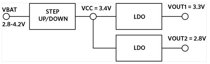
Figure 1. LDO input voltage set by the step-up/step-down converter
In portable applications, the higher the efficiency, the longer the working time, so the regulator efficiency is the most important. This article reviews the options available, compares their performance, and identifies the most efficient solution.
One way to bypass / boost solve this problem is to use a bypass / boost converter, boost converter is external with the "bypass" transistor; integrated power transistor (the VBAT) and LDO input (VCC )between. Figure 2 shows the bypass/boost power chain structure and its operation table. The bypass transistor T3 performs an "inefficient" step-down operation. 20160702fig2
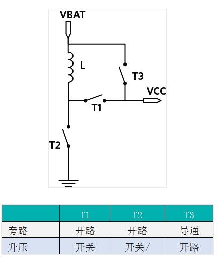
Figure 2. Bypass/Boost Power Supply Chain and Operation Table
This configuration can only regulate VBAT voltages below the set VCC = 3.4V. If VBAT > 3.4V, the boost converter stops regulating and the pass transistor turns on, connecting VBAT directly to VCC. Figure 3 shows the battery discharge characteristics and the LDO input voltage in the bypass/boost configuration.
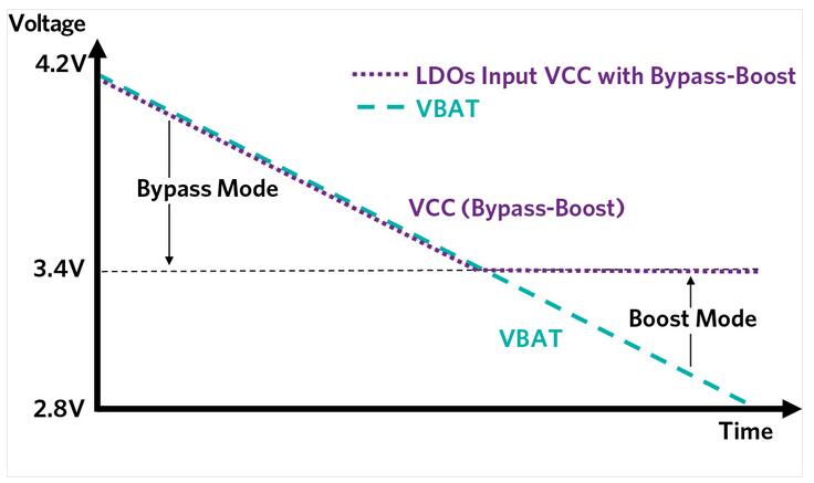
Figure 3. LDO input voltage characteristics for bypass/boost operation
Most of the time (VBAT > 3.4V), the pass transistor in the bypass/boost configuration "passes" the input voltage to the downstream LDO circuit as it is. The LDO is responsible for stepping down the high VBAT value to its output setpoint. Since this adjustment process is linear, the power consumption inside the LDO is high. This results in higher energy consumption and also requires board design and IC selection to dissipate this energy consumption.
The buck /boost converter used in this circuit regulates its output to 3.4V from start to finish compared to the bypass/boost configuration. In addition, the voltage regulation process is completely switch mode, and the work efficiency is high. Figure 4 shows the structure of the step-up/step-down power chain and its operation table.
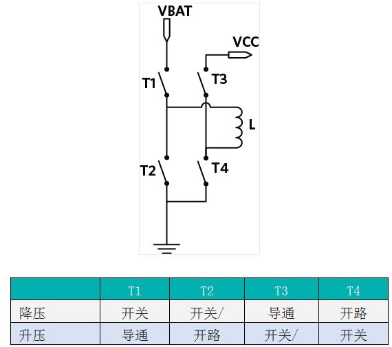
Figure 4. Step-up/step-down power chain and operation table
When VBAT > VCC, the IC operates in the Buck mode; when VBAT < VCC, it smoothly transitions to the Boost mode. Covers the entire battery voltage range with high efficiency, switching mode. Figure 5 shows the battery discharge characteristics and the LDO input voltage in the step-up/step-down configuration.
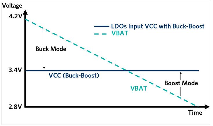
Figure 5. LDO input voltage characteristics for up/down operation
In Figure 6, the two modes of operation are superimposed, and in the shaded portion, the power consumption of the boost/buck mode has significant advantages. The shaded triangle area represents the power loss when the bypass/boost operation is linearly regulated.
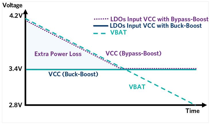
Figure 6. Comparison of LDO input voltage characteristics in up/down and bypass/boost modes
In the case study case study, we compared the Maxim MAX77801 liter/buck IC to a competitor's bypass/boost IC. Each regulator drives a single 3.3V LDO with a load current of 500mA.
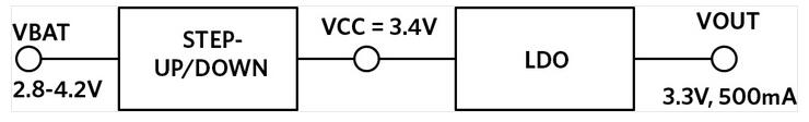
Figure 7. Efficiency test configuration
Figure 8 shows the comparison results. The solid line indicates the efficiency of each scheme, and the broken line indicates its battery current loss. As expected, the efficiency of the two structures is similar when VBAT is below or close to the LDO output voltage; outside of this range, the efficiency of the buck/b structure is greater than 90% over the entire time that VBAT is above the LDO output voltage. ) far superior to the efficiency of the bypass/boost structure (down to 67% at full battery charge). This excellent performance is due to the ability of the step-up/step-down IC to power the LDO in switch mode over the entire operating range.
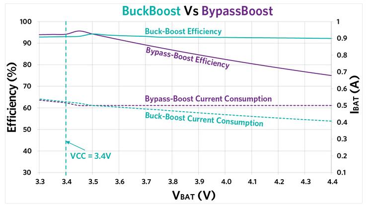
Figure 8. Efficiency comparison of up/down and bypass/boost structures
Conclusion The comparison of the buck-boost structure with the bypass/boost structure demonstrates that the buck-boost mode of operation is inherently superior. By comparing the MAX77801 liter/buck solution with the competitor's bypass/boost architecture, the results show that Maxim devices are up to 25% more efficient. Therefore, the step-up/step-down IC is an ideal solution for portable applications.
Coalbed Gas Generator,Diesel Water Pump Generator,Diesel Geneator Water Pump,Silent Gas Generator
Jiangsu Vantek Power Machinery Co., Ltd , https://www.vantekpower.com