![<?echo $_SERVER['SERVER_NAME'];?>](/template/twentyseventeen/skin/images/header.jpg)
The manufacturing process of the LED chip can be roughly divided into several steps such as a wafer processing process (Wafer FabricaTIon), a wafer needle testing process (Wafer Probe), a packaging process (Packaging), and a test process (IniTIal Test and Final Test). The wafer processing step and the wafer needle measurement step are the front end steps, and the assembly process and the test process are the back end processes.
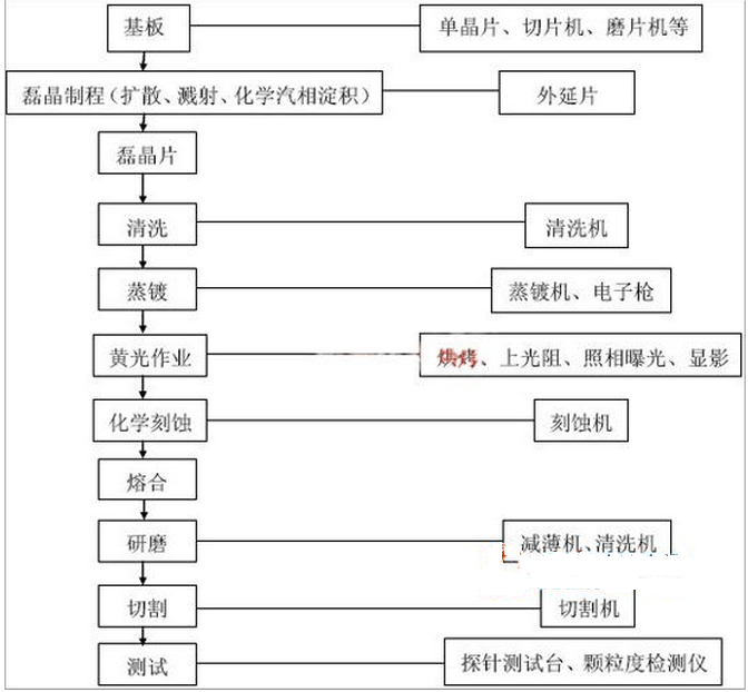
1, wafer processing process
The main work of this process is to make circuits and electronic components (such as transistors, capacitors, logic switches, etc.) on the wafer. The processing procedure is usually related to the product type and the technology used, but the general basic procedure is to first properly apply the wafer. After cleaning, oxidation and chemical vapor deposition are performed on the surface, and then repeated steps such as coating, exposure, development, etching, ion implantation, and metal sputtering are performed, and finally, several layers of circuits and components are processed and fabricated on the wafer.
2, wafer needle testing process
After the previous process, a small grid, ie, a die, is formed on the wafer. Generally, in order to facilitate testing and improve efficiency, the same type and specification of products are produced on the same wafer; Need to make several products of different varieties and specifications. After measuring the electrical characteristics of each die with a probe, and marking the unqualified die, the wafer is cut and divided into individual grains, and then according to their electrical characteristics. Classification, loading into different trays, and rejecting unqualified grains.
3, the assembly process
That is, a single die is fixed on a plastic or ceramic chip base, and some lead terminals etched on the die are connected with the pins protruding from the bottom of the base to be connected to the external circuit board. Finally, cover the plastic cover and seal it with glue. Its purpose is to protect the crystal grains from mechanical scratches or high temperature damage. At this point, we have made an integrated circuit chip (that is, those black or brown that we can see in the computer, rectangular blocks with many pins or leads on both sides or four sides).
4, the test process
The last process of chip manufacturing is testing, which can be divided into general testing and special testing. The former is to test the electrical characteristics of the packaged chip under various environments, such as power consumption, running speed, and withstand voltage. The tested chips are classified into different grades according to their electrical characteristics. The special test is based on the technical parameters of the customer's special needs, taking some chips from similar parameter specifications and varieties, and doing targeted and specific tests to see if they can meet the special needs of customers to decide whether they must design special for customers. chip. After the products that have passed the general test are affixed with the labels of the specifications, models and date of manufacture, and then packaged, they can be shipped. Chips that fail the test are classified as downgrades or scraps depending on the parameters they reach.
LED chip manufacturing process:
Epitaxial wafer→cleaning→plating transparent electrode layer→transparent electrode pattern lithography→corrosion→debonding→platform pattern lithography→dry etching→debonding→annealing→SiO2 deposition→window pattern lithography→SiO2 corrosion→degglomerate→ N-pole pattern lithography → pre-cleaning → coating → stripping → annealing → P-pole pattern lithography → coating → stripping → grinding → cutting → chip → finished product test.
LED chip manufacturing process
In fact, the production process of the epitaxial wafer is very complicated. After the epitaxial wafer is finished, the next step is to make electrodes (P-pole, N-pole) for the LED epitaxial wafer, and then start cutting the LED epitaxial wafer with a laser machine (previously cutting LED epitaxial wafers are mainly made of diamond knives. After being fabricated into chips, nine points are taken at different positions on the wafer for parameter testing.
1. Test the voltage, wavelength and brightness mainly. The wafer that meets the normal shipping standard parameters will continue to do the next step. If the nine-point test does not meet the relevant requirements, the wafer is placed on one side. deal with.
2. After the wafer is cut into chips, 100% visual inspection (VI/VC), the operator should use a microscope magnified 30 times for visual inspection.
3. Then use the fully automatic sorter to fully automate the selection, testing and classification of the chips according to different voltage, wavelength and brightness prediction parameters.
4. Finally, check (VC) and label the LED chip. The chip area should be at the center of the blue film. There are up to 5,000 chips on the blue film, but the number of chips on each blue film must be no less than 1000. The chip type, batch number, quantity and photoelectric measurement statistics are recorded on the label. Attached to the back of the glossy paper. The chip on the blue film will be the same as the first visual inspection standard, ensuring that the chips are neatly arranged and of good quality. This makes LED chips (currently known as square chips on the market). In the process of manufacturing the LED chip, some defective or electrode-worn chips are separated. These are the latter crystals. At this time, there are some wafers on the blue film that do not meet the normal shipping requirements. Become a side piece or a piece of hair.
I just talked about extracting nine points at different positions on the wafer for parameter testing. For wafers that do not meet the relevant requirements, these wafers cannot be directly used as LED chips, and they do not do anything. After the inspection, it was sold directly to the customer, which is the LED wafer on the market (but there are also good things in the big wafer, such as square chips).
Wuxi Doton Power , https://www.dotonpower.com