![<?echo $_SERVER['SERVER_NAME'];?>](/template/twentyseventeen/skin/images/header.jpg)
Timing analysis is available in ISE and timing analysis is also available in PlanAhead. The steps for timing analysis with PlanAhead are described below.
First, the operation timing analysis
1. Run [File] → [Open Project] in PlanAhead and open the following project, PlanAhead_Tutorial/Projects/project_cpu_netlist/project_cpu_netlist.ppr, and the [Floorplan] window shown in Figure 10-66 will appear.
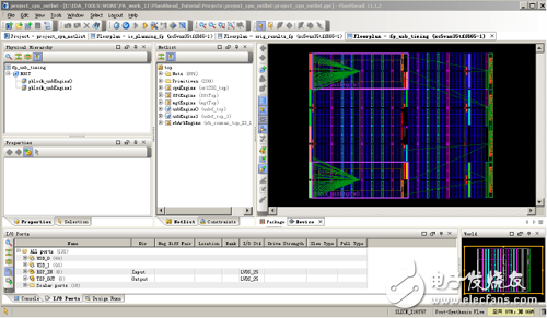
Figure 10-66 PlanAhead's Floorplan view
2. Select the Floorplan – orig_results_fp tab.
3. Run [Tools] → [Run TImeAhead] to open the dialog box shown in Figure 10-67 and set the timing analysis related properties. Set up as shown in the figure and click [OK] to start timing analysis.
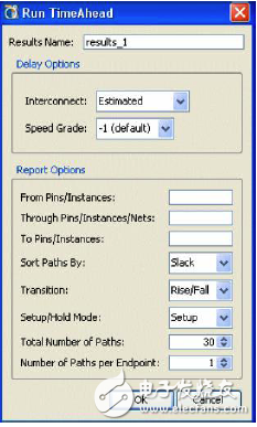
Figure 10-67 Timing Analysis Attributes
4. The analysis is completed and the timing analysis results are shown in Figure 10-68. The figure shows the timing type, margin, source/destination object, total delay, logic delay, network line delay percentage, and logic level.
![Timing Analysis Results [Timing Results]](http://i.bosscdn.com/blog/06/16/12/W07_0.png)
Figure 10-68 Timing Analysis Results [TIming Results]
The red color in the figure is the path of the timing violation, which needs to be checked and corrected by the designer.
5. Select the Path1 path and maximize the [ProperTIes] window. As shown in Figure 10-69, you can see the details of the path, including the source clock path, destination clock path, and data path. The composition of the path and the component delay and network delay information.
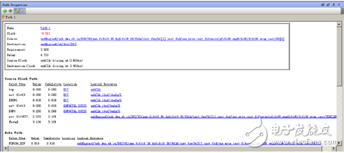
Figure 10-69 Timing path properties
Second, detect the timing path in the [SchemaTIc] view.1. Display schematic structure 1.
In the [Timing Results] window, select [Schematic] from the right-click pop-up menu of the Path1 path to open the schematic structure view as shown in Figure 10-70.
2. Display schematic structure 2.
In the [From] column of the [Timing Results] window, select all the paths starting with usbEngine0/..., right-click and select [Schematic] from the pop-up menu to open the schematic view of multiple timing paths shown in Figure 10-71.
3. Display the hierarchy.
Select [Select Primitive Parents] in the right-click menu of the [Schematic] window in Figure 10-71, and select [Show Hierarchy] in the right-click menu again. The design module containing the two partial logics shown in the [Schematic] window will be displayed. In the [Hierarchy] window. As shown in Figure 10-72.
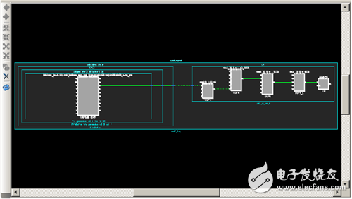
Figure 10-70 Schematic path schematic view
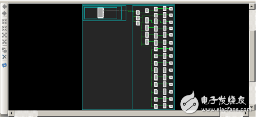
Figure 10-71 Schematic view of multiple timing paths
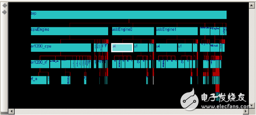
Figure 10-72 Hierarchical view
Third, edit the timing constraints1. Change the TS_cpuClk period constraint from 11.75ns to 11.5ns.
In Figure 10-73, select the [Constraits] tab next to the [Netlist] tab, select the TS_cpuClk constraint shown in the figure, and see the related properties of this constraint in the [Constraint Properties] property window. Here you can edit the constraints. Name, period, duty cycle, grouping, and priority. Here only need to change 11.75ns to 11.5ns, then an [Apply] button will appear in the [Constraint Properties] property window, click to complete the constraint modification.
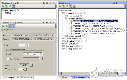
Figure 10-73 Modifying timing constraints
2. Create a new timing constraint.
Click on the [Constraint] window in Figure 10-74 to bring up the [Create New Timing Constraint] dialog box. You can select a constraint type and add a new timing constraint.
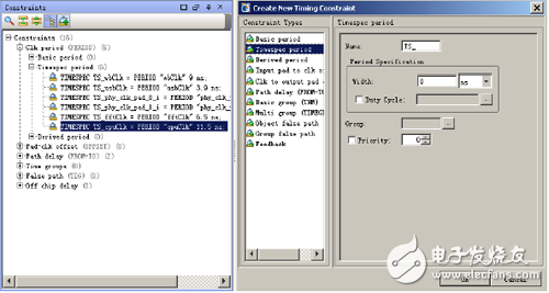
Figure 10-74 New timing constraint
3. Remove timing constraints.
Select a timing constraint in the [Constraint] window and press the [Del] button to delete the constraint.
Qi Charger,Wireless Charger,Wireless Phone Charger,Wireless Charging Station
wzc , https://www.dg-wzc.com