![<?echo $_SERVER['SERVER_NAME'];?>](/template/twentyseventeen/skin/images/header.jpg)
Cadence is a large EDA software that performs almost every aspect of electronic design, including ASIC design, FPGA design, and PCB board design. Cadence has absolute advantages in simulation, circuit diagram design, automatic placement and routing, layout design and verification. Cadence contains more tools that cover almost every aspect of EDA design. Here's how to teach Cadence to build a PCB.
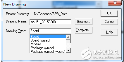
Cadence builds PCB steps1. Open PCB Editor-"Allegro PCB Design GXL
2, File-"New
Where Board (wizard) builds the PCB for the wizard
File-》Save As Change PCB storage path
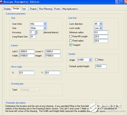
3, Setup-"Design Parameter...
Set the unit of use, the size of the drawing, the unit precision, and the working area (where Left X and Lower Y indicate the coordinates of the lower left corner, and set to a negative value so that the origin of the coordinates is inside the working area)
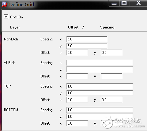
4, Setup-"Grids...
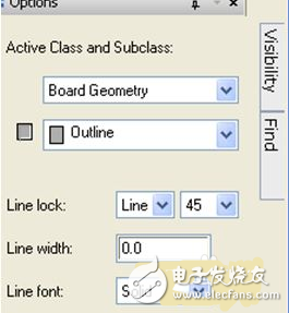
5, add the board frame: Add-"Line
Select the default settings, note that the opTIon options Class and Subclass must be as shown below
Manual addition: If there is no clear size requirement, you can manually add a rectangular frame in the work area (Line lock is set to 90°). After the PCB design is completed, adjust the size according to the actual situation.
Coordinate input: Enter x 0 0 Enter, ix 10000 Enter, iy 10000 Enter, ix -10000 Enter, iy -10000 Enter, and the right mouse button Done to complete the operation. The frame size is set according to actual needs or PCB size.
The Cadence software cannot directly modify the size of the board frame. It can only be deleted and added again.
6. Add chamfer: Manufacture-"DrafTIng, where Fillet (circle), Chamfer (straight line).
Select Add Round Chamfer: Radius (the chamfer size) in opTIon is set to 100mil, and the mouse clicks on the two lines that need to be added chamfer, and the addition is completed. If the size is uncertain, it can be added after the PCB design is completed.
7. Place the fixing holes: Place-》Manually (Check Library in Advanced SetTIngs)
Select the Mechanical symols from the Placement List drop-down menu, select MTG125 (inner diameter 125mil), and place the corresponding coordinates in the command window on the four corners of the PCB.
Fixed mounting holes: Edit->Property Select the target, select fixed, Apply, OK.
8, regional settings: Setup-"Areas (not required)
Package Keepin: Allow placement area
Package Keepout: Prohibited placement area
Route Keepin: Allow wiring area
Route Keepout: Prohibited wiring area
Ev Charging Cable,Electric Car Charging Cable,Type 2 Charging Cable,32A Ev Charging Cable
Yangzhou JERI New Energy Co., Ltd. , https://www.jrevcharging.com