![<?echo $_SERVER['SERVER_NAME'];?>](/template/twentyseventeen/skin/images/header.jpg)
The DS12C887 real-time clock chip is rich in functionality and can be used to directly replace the clock calendar chip DS12887 on the IBM PC. At the same time, its pins are also compatible with MC146818B and DS12887.
Since the DS12C887 can automatically generate time information such as years, years, months, days, hours, minutes, seconds, and so on, it has added a century register internally, thereby using the hardware circuit to solve the "millennium" problem; DS12C887 comes with a lithium battery, external In the event of a power failure, its internal time information can also be maintained for 10 years; for time records in the day, there are 12 hours and 24 hours modes. In the 12-hour mode, AM and PM are used to distinguish between AM and PM. There are also two ways to represent time. One is represented by a binary number, and the other is represented by a BCD code. The DS12C887 has a 128-byte RAM. The 11-byte RAM is used to store time information. The 4-byte RAM is used to store the control information of the DS12C887, which is called the control register. The 113-byte general-purpose RAM allows the user to use it. In addition, the user can also program the DS12C887 to realize a variety of square waves. Output, and its internal three-way interrupt can be masked by software.
2 pin function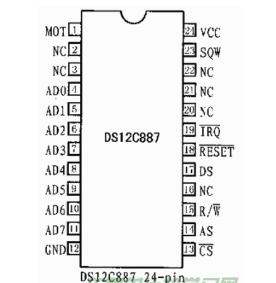
The pin arrangement of DS12C887 is shown in Figure 1. The function of each pin is described as follows:
GND, VCC: DC power supply, where VCC is connected to the +5V input and GND is grounded. When the VCC input is +5V, the user can access the data in the RAM in the DS12C887 and can read and write the data. When the VCC input is less than When +4.25V, the user is prohibited from reading or writing internal RAM. At this time, the user cannot correctly obtain the time information in the chip. When the input of VCC is less than +3V, DS12C887 will automatically switch the power supply to the internal lithium battery. In the pool, to ensure that the internal circuits can work properly.
MOT: Mode selection pin, DA12C887 has two operating modes, Motorola mode and Intel mode. When MOT is connected to VCC, the selected working mode is Motorola mode. When MOT is connected to GND, the Intel mode is selected. This article focuses on Intel mode.
SQW: square wave output pin. When the supply voltage VCC is greater than 4.25V, the SQW pin can be used for square wave output. At this time, the user can obtain 13 types of square wave signal output by programming the control register.
AD0 ~ AD7: Multiplexes the address data bus, this bus adopts the time division multiplexing technology, in the first half of the bus cycle, it is the address information that appears on AD0- AD7, can use to strobe the RAM in DS12C887, the second half of bus cycle Part of the data appears on AD0 ~ AD7.
AS: Address strobe input pin. During read and write operations, the rising edge of AS latches the address information appearing on AD0~AD7 to DS12C887, and the next falling edge clears the address information on AD0~AD7, regardless of whether Effective, DS12C887 will perform this operation.
DS/RD: Data selection or read input pin. This pin has two operating modes. When MOT is connected to VCC, Motorola operating mode is selected. In this working mode, the DS of the rear part of each bus cycle is high power. Flat, known as data strobe. During a read operation, the rising edge of DS causes the DS12C887 to send internal data to buses AD0 through AD7 for external reads. During a write operation, the falling edge of DS will latch data on AD0~AD7 in DS12C887. When MOT is connected to GND, the Intel operating mode is selected. In this mode, this pin is the read enable input pin, ie Read. Enable.
R/W: Read/write input. This pin also has two operating modes. When MOT is connected to VCC, R/W operates in Motorola mode. At this time, the function of this pin is to distinguish between read operation and write operation. When R/W is high, it is a read operation. When R/W is low, it is a write operation. When MOT is connected to GND, the pin is Work in Intle mode, this time as a write enable input, that is, Write Enable.
CS: chip select input, active low.
IRQ: Interrupt request input, active low, this pin has no effect on the contents of the clock, calendar, and RAM in the DS12C887. It only affects the internal control registers. In a typical application, RESET can be directly connected to VCC. This ensures that the DS12C887's internal control registers are not affected when power is lost.
There are 11 bytes of RAM in the DS12C887 to store time information and 4 bytes to store control information. The specific scale addresses and values ​​are listed in Table 1.
Can be found out from Table 1: There are 4 control registers such as AB of the control register inside DS12C887, users can visit it at any time to carry on control operation to DS12C887.
Table 1 DS12C887 storage function
Address Function Value Range Decimal value Range of value Binary BCD code 0 seconds 0 to 5900 to 3B00 to 591 seconds Alarm 0 to 5900 to 3B00 to 592 minutes 05900 to 3B00 to 593 minutes Alarm 0 to 5900 to 3B00 to 59412 Hour mode 0~1201~0C AM,
81~8C PM01~12AM,
81~92PM 24 hours mode 0~2300~1700~ 235 hours alarm, 12 hour system 1~1201~0C AM,
81~8C PM01~12AM,
Alarm clock from 81 to 92 PM, 24-hour clock 0 to 2300 to 1700 to 236 days of the week (Sunday=1) 1 to 701 to 0701 to 077 days 1 to 3101 to 1F01 to 318 months 1 to 1201 to 0C01 to 129 years 0 to 9900~6300~9910 Control Register A
11 control register B
12 control register C
13 control register D
50th century 0~99NA19,20
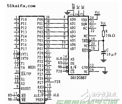
3 ApplicationIn various devices, home appliances, instruments, and industrial control systems, it is easy to use the DS12C887 to form a time acquisition unit to achieve various time acquisitions. Figure 2 is a time acquisition circuit consisting of an 8031 ​​single-chip microcomputer and DS12C887. The base address of the DS12C887 is 7F00H, and the corresponding program is written in C51 language (taking the Intel operating mode as an example).
The initialization procedure for the time acquisition circuit formed by the 8031 ​​microcontroller and the DS12C887 is as follows:
XBYTE[0x7F00+0x0B]=0x82;
XBYTE[0x7F00+0x0A]=0xA0;
XBYTE[0x7F00+0x0A]=0x20;
XBYTE[0x7F00+0x0B]=0x02;
/* All interrupts are prohibited, 24-hour clock, BCD code mode */
The following are all time programs:
Unsigned char data t-century;
Unsigned char data t-year;
Unsigned char data t-month;
Unsigned char data t-date;
Unsigned char data t-week;
Unsigned char data t-hour;
Unsigned char data t-minute;
Unsigned char data t-second;
If((XBYTE[7F00+0x0A]&0x80)!=0){
T-century=XBYTE[0x7F00+0x32];/*read century*/
T-year=XBYTE[Ox7F00+0x09];/*read year*/
T-month=XBYTE[Ox7F00+0x08];/*read month*/
T-date=XBYTE[Ox7F00+0x07];/*read date*/
T-week=XBYTE[Ox7F00+0x06];/*Read day of week*/
T-hour=XBYTE[Ox7F00+0x04];/*reading hour*/
T-minute=XBYTE[DS12887+0x02];/*read minute*/
T-second=XBYTE[Ox7F00+0x00];}/*read seconds*/
4 ConclusionDallas's clock calendar chip DS12C887 is feature-rich, easy to use, and highly likely to be a good choice for time-producing circuits.
Fine Steel Cord For PU Timing Belts
Fine Steel Cord For PU Timing Belts
PU Timing Belts with steel cord, Timing belts truly endless or Jointed endless with cleats, for conveyor and Transmission Purpose
Our firm is providing an extensive series of PU Timing Belt with Steel Cord. Professionals use top quality material, which is sourced from truthful sellers of market to make this product. Our clientele can attain this product in varied specifications that meet on their necessities. Quality checkers also check this product on definite quality standards before delivery to the patrons.
Fine Steel Cord,Fine Steel Wire Rope,Pu Belt Steel Cord,Pu Timing Belt With Steel Cord
ROYAL RANGE INTERNATIONAL TRADING CO., LTD , https://www.royalrangelgs.com