![<?echo $_SERVER['SERVER_NAME'];?>](/template/twentyseventeen/skin/images/header.jpg)
**0. Preface**
In modern automatic control systems, the parameters that need to be measured and controlled are often continuous analog signals such as temperature, pressure, flow rate, and speed. These physical quantities are typically represented as continuously varying voltages or currents. To be processed by digital computers, they must first be converted into digital signals through an analog-to-digital (A/D) conversion process. Once in digital form, these signals are processed within the computer to generate a digital control signal. This signal is then converted back to an analog voltage or current using a digital-to-analog (D/A) converter and sent to an actuator to drive the corresponding device. This allows for precise and automated control of industrial processes.
**1. Main Features and Working Principles of TLC549**
**1.1 Key Features of TLC549**
The TLC549 is an 8-bit serial analog-to-digital converter (ADC) that uses CMOS technology and operates based on a switched-capacitor architecture. It can be easily interfaced with microprocessors and controllers via three communication lines: I/O CLOCK, CS (Chip Select), and DATAOUT. The chip has an internal system clock running at 4 MHz, with a maximum conversion time of 17 microseconds and a maximum sampling rate of 40,000 samples per second. It features a total offset error of up to ±0.5 LSB and typical power consumption of only 6 mW.
The TLC549 includes a high-impedance differential reference voltage input, which helps reduce noise interference and allows for calibration of the conversion range. Due to its VREF grounding, where the difference between VREF+ and VREF- is at least 1V, it is well-suited for sampling small signals. Additionally, the device operates on a single power supply ranging from 3V to 6V. Overall, the TLC549 offers advantages such as minimal control pins, simple timing requirements, fast conversion speed, low power consumption, and cost-effectiveness. It is ideal for use in low-power portable devices and can also be connected in parallel with multiple units.
The internal block diagram and pin configuration of the TLC549 are illustrated in Figure 1.
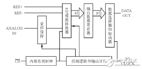
Figure 1: Internal block diagram and pin names of TLC549
**1.2 Absolute Maximum Ratings of TLC549** The absolute maximum ratings for the TLC549 are as follows: - **Power Supply Voltage:** 6.5 V - **Input Voltage Range:** 0.3 V to VCC + 0.3 V - **Output Voltage Range:** 0.3 V to VCC + 0.3 V - **Peak Input Current (Any Input Terminal):** ±10 mA - **Peak Input Current (All Inputs):** ±30 mA - **Operating Temperature:** - TLC549C: 0°C to 70°C - TLC549I: -40°C to 85°C - TLC549M: -55°C to 125°C These specifications ensure the device can operate reliably under a wide range of environmental conditions.Fiber Optical Tools,Fiber Optic Termination Tool Kit,fiber Visual Fault Locator,Optical Fiber Length Fixer,gpon sfp module
Shenzhen Runtop Technology Co.LTD , https://www.runtoptech.com