With the acceleration of Taiwan's upstream transfer capacity to mainland China and the active expansion of local Chinese companies, China's LED chip market will usher in more intense competition and the market will become more unpredictable.
For a long time, the High-tech LED Industry Research Institute (GLII) closely tracks the industry dynamics of LED upstream. Based on the "2011 China LED upstream industry research report" released by the High-tech LED Industry Research Institute (GLII), combined with the actual research on the upstream epitaxial chip companies in the country, in January 2012, the high-tech LED industry research institute (GLII) ) The 2012 China LED upstream industry research report was compiled.
This report provides a detailed analysis and forecast of the market conditions of China's upstream sapphire substrate, MO source, MOCVD, epitaxial wafer, chip, enterprise, industrial policy, investment risk, investment prospects, etc., for LED peers and caring LED upstream industry. People for reference.
To purchase the above report, please contact the contact person: Mr. Zhang Tel: 0755-26981898-839
Email: hb.

table of Contents
Chapter I Overall Analysis of China's LED Upstream Industry 4
Section 1 In 2011, China's LED upstream staged overheated investment 4
Section 2 Analysis of China's LED upstream industry competition situation 8
Section III Main Features of China's LED Upstream Industry 10
Chapter II Analysis of China LED Chip Enterprise Development 16
Section 1 The number of Chinese LED chip companies is growing rapidly 16
Section 2 Analysis of the time and mass production time of Chinese LED chip companies in each year 26
Section III Analysis of Regional Distribution of Chinese LED Chip Enterprises 31
Section IV Analysis of Source Types of Chinese LED Chip Enterprises' Funds 45
Section V Investment Analysis of Taiwanese-funded Enterprises in China's LED Chips 51
Section VI Investment Analysis of Other Foreign-funded Enterprises in China's LED Chip Industry 55
Chapter III Analysis of China LED Chip Market 58
Section 1 Market Size Analysis of China's LED Chip Industry 58
Section 2 Sales Analysis of Chinese LED Chip Enterprises 59
Section III Analysis of China LED Chip Enterprise Chip Types 61
Chapter IV Market Analysis of China's LED Epitaxial Film 64
Section 1 China LED Epitaxial Film Market Analysis 64
Section 2 Analysis of China LED Epitaxial Film Market Development Trends 65
Chapter 5 MOCVD Analysis in China's LED Industry 67
Section 1 MOCVD quantitative analysis of China's LED industry 67
Section 2 MOCVD quantitative analysis of each LED chip company 67
Section III MOCVD Market Supply Analysis 72
Section 4 Global MOCVD Overall Market Capacity Forecast 78
Chapter VI China LED Sapphire Substrate Market Analysis 79
The first section of the 2010 global sapphire substrate is seriously short of material, 2011 sapphire oversupply 79
Section 2 Global Sapphire Substrate Major Manufacturers Analysis 80
Section III Market Demand Analysis of Chinese Sapphire Substrate 90
Section IV Market Description of Silicon Carbide Substrate 91
Chapter VII Analysis of China's MO Source Market 93
Section 1 Status and Forecast of Demand for China's MO Source Markets 93
Section 2 Analysis of MO Source Photoelectric Material Industry Chain 96
Section III Market Characteristics of MO Source Photoelectric Materials 98
Section IV Analysis of Major Manufacturers of Global MO Sources 98
Chapter VIII Analysis of China's LED upstream equipment 103
Section 1 Analysis of Major Suppliers of China's LED Upstream Equipment 103
Section 2 Localization Analysis of China's LED Upstream Equipment 106
Chapter IX China's LED upstream industry related policy analysis 111
Section 1 China's National LED Industry Support Policy 113
Section 2 Relevant Policies of Local Cities in China 119
Chapter 10 China LED Chip Key Enterprises and Latest Projects 131
Section I Introduction of Key Enterprises 131
Section 2 China 2011 New LED Chip Related Projects Introduction 154
Chapter XI China LED upstream industry development forecast 160
Chapter Twelve Analysis of Investment Risks and Investment Prospects of China's LED Upstream Industry 164
Section 1 Major Investment Risks of China's LED Upstream Industry 164
Section 2 LED upstream industry investment advice 168

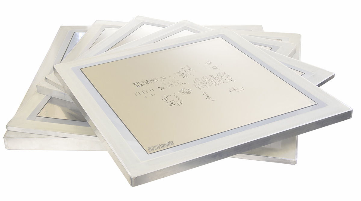
PCB SMT Stencil ,the unique goal is to move solder paste to the bare Printed Circuit Board.
PCB Stencil , SMT Stencil, SMD Stencil , Laser Stencil , What is it?
Apart from all types of Printed Circuit Boards (PCBs) such as Prototype PCB , Aluminum PCB , HDI PCB , Flexible PCB , Rigid Flex PCB , Thick Copper PCB, High TG PCB , JHYPCB also manufactures solder paste stencils to meet Surface Mount Technology (SMT) requirements.
PCB Stencils, also called SMT stencils, SMD stencil, play a key role in transferring accurate amount of solder paste to correct positions on bare circuit boards ready for assembly. In other words, stencils can fast and efficiently ensure the most accurate solder paste amount and optimal electrical connection. With solder stencils, it is possible to use metal squeegee blades to apply solder paste easily over the openings on PCBs and make stencil to be well aligned with the surface of the advanced circuit board.
All of our SMT Stencils stencils are 100% laser-cut type 304 full-hard stainless steel, ensuring the finest quality finish on the market today. We use a .001" laser beam with 98% overlap creating an extremely smooth hole that provides the best paste release. Most stencil fabricators use a .003" laser leaving mouse bites on the aperture edge. You can choose a PCB Prototype stencil, a frameless foil stencil, or a rigid permanently mounted stencil. Both the frameless and framed stencils come in various sizes to accommodate your printer and stencil requirements.
PCB Stencil Types Available:
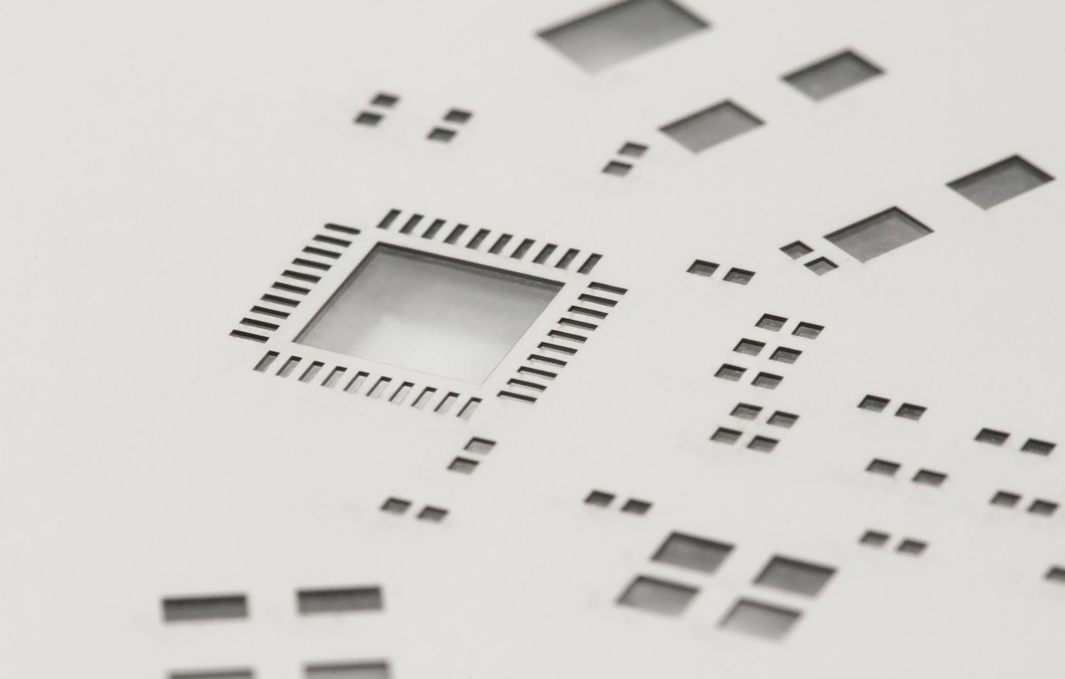
1. Laser-cut stencils
The openings are lasered on 100% stainless steel. Generally speaking, this kind of stencil can be produced with high quality and a high degree of precision within a short time.
- Advantages: high accuracy; barely influenced by objective elements; trapezoid opening beneficial for demoulding; suitable for accurate cutting; reasonable price;
- Disadvantages: relative low manufacturing speed.
2. Chemical-etch stencil
The openings are etched into the metal using acid. Usually this kind of stencil offers better protection on material temper and hardness.
- Advantages: one-time formation; relatively high manufacturing speed; low cost;
- Disadvantages: tending to form sand clock shape or large openings; numerous manufacturing stages and accumulating errors; unsuitable for fine pitch stencils; bad for environmental protection.
3. Prototype PCB Stencil (Low-volume manual printing. Ideal for prototypes)
When prototyping dictates fast action with minimal cost, our prototype stencils are the best solution. Prototype Stencils gives you a quality stencil and framework so you can handle assembly from the convenience of your own desk.
Prototype SMT Stencil Features:
- Eliminate the registration difficulty associated in hand printing with a flat piece of metal
- Eliminate printer set up for short run prototypes
- Allow quick alignment for repeatability
- Save money over full size stencils designed for automated printers<
- Squeegee included
| Prototype SMT Stencil Specs: | |
| Technology | 100% laser cut |
| Material Used | Stainless Steel |
| Stencil Thickness | 0.06 ~ 0.3 mm |
| Minimum Cut Width | 0.05 mm |
| Maximum Size | 736 X736 mm |
| Aperture Tolerance | within 0.007mm |
| Allow for Fiducial Data | Yes |
| Delivery | 1 ~2 Day |
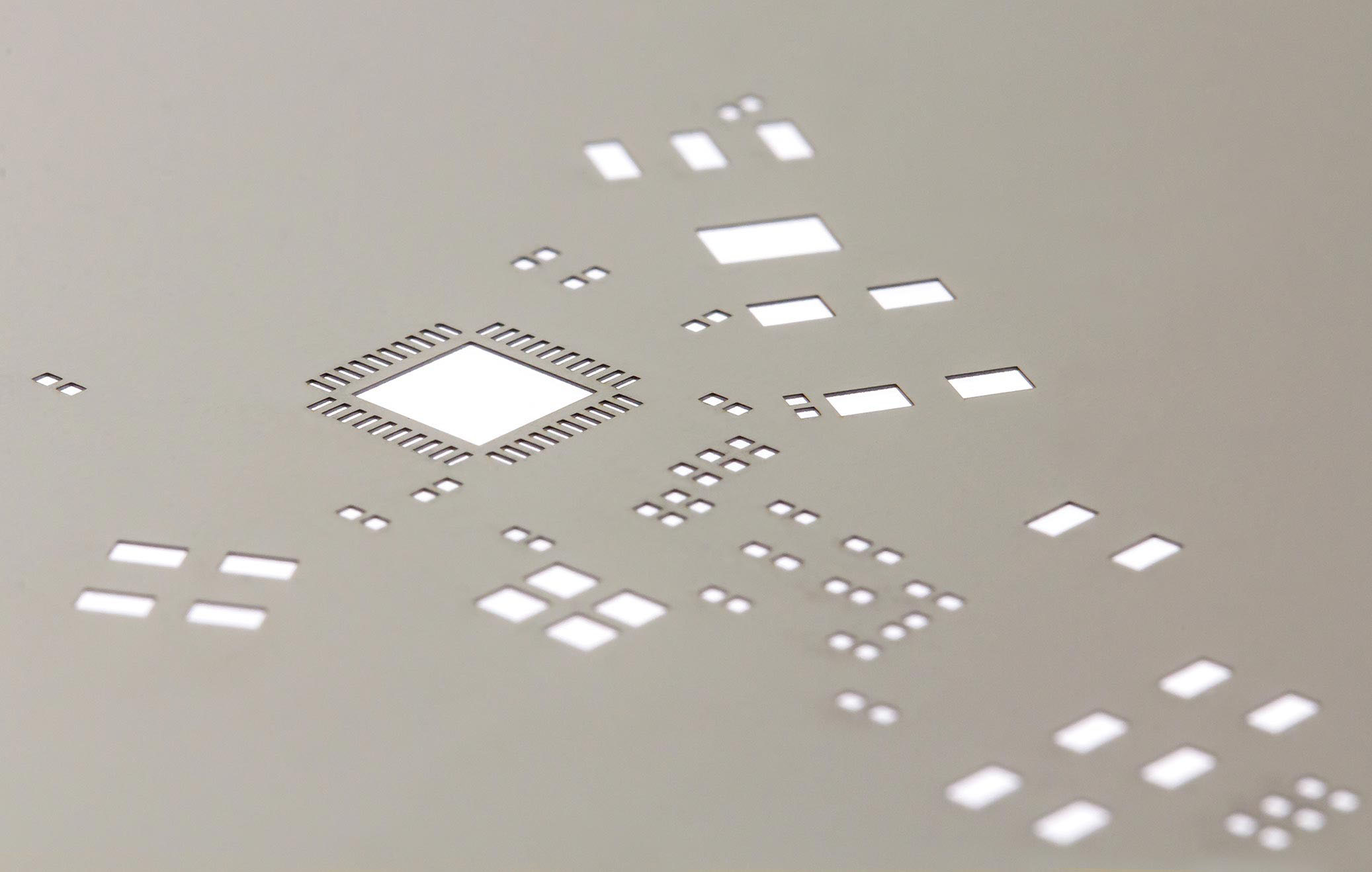
4. NEW Prototype PCB Stencil Kit (with leaded or lead/free solderpaste)
Includes Prototype Stencil, one board holder, leaded or lead-free solder paste (must specify), temperature marker, squeegee, ESK-safe gloves and alcohol wipe.
5. NEW Pick and Place Tool
Handy and convenient for low quantity prototype assembly using the Prototype Stencils. Re-usable, includes vacuum bulb and vacuum clips with diameters of 3/8", 1/4", and 1/8".
6. Framed SMT Stencils (Also called "Glue-in" or Mounted Stencils)
Framed stencils are laser-cut stencils designed for high volume screen-printing. With a framed stencil, your stencil is securely mounted to either a cast or extruded aluminum stencil frame a stencil frame using a mesh border, allowing for complete control.
Framed SMT Stencil Features:
- Unique Process for smooth aperture walls
- Very clean laser-cut apertures
- Excellent print performance
- Excellent for high-volume stencil printing on printed circuit boards
- Unique process creates permanent non-removable non-fading fiducial
- All framed SMT stencils are double bonded to extreme wear
- 24-hour turnaround standard
| Framed SMT Stencil Specs: | |
| Technology | 100% laser cut |
| Material Used | Stainless Steel |
| Frame Types | Cast, Space Saver |
| Stencil Thickness | 0.06 ~ 0.3 mm |
| Minimum Cut Width | 0.05 mm |
| Maximum Size | 736 X736 mm |
| Aperture Tolerance | within 0.007mm |
| Allow for Fiducial Data | Yes |
| Allow for Panelized Data | Yes |
| Delivery | 1 ~2 Day |
Framed PCB Stencil Specification
|
Framed PCB Stencil Area |
Maximum Squeegee Area |
|
300mm*400mm (11.81inch*15.75inch) |
120mm*220mm (4.72inch*8.66inch) |
|
370mm*470mm (14.57inch*18.5inch) |
200mm*300mm (7.87inch*11.81inch) |
|
400mm*600mm (15.75inch*23.62inch) |
220mm*400mm (8.66inch*15.75inch) |
|
400mm*700mm (15.75inch*27.56inch) |
220mm*500mm (8.66inch*19.69inch) |
|
400mm*800mm (15.75inch*31.5inch) |
220mm*600mm (8.66inch*23.62inch) |
|
400mm*900mm (15.75inch*35.43inch) |
220mm*700mm (8.66inch*27.56inch) |
|
400mm*1000mm (15.75inch*39.37inch) |
220mm*800mm (8.66inch*31.5inch) |
|
400mm*1200mm (15.75inch*47.24inch) |
220mm*1000mm (8.66inch*39.37inch) |
|
400mm*1400mm (15.75inch*55.12inch) |
220mm*1200mm (8.66inch*47.24inch) |
|
420mm*520mm (16.54inch*20.47inch) |
240mm*340mm (9.45inch*13.39inch) |
|
450mm*550mm (17.72inch*21.65inch) |
270mm*370mm (10.63inch*14.57inch) |
|
500mm*800mm (19.69inch*31.5inch) |
320mm*600mm (12.6inch*23.62inch) |
|
500mm*1200mm (19.69inch*47.24inch) |
320mm*1000mm (12.6inch*39.37inch) |
|
550mm*650mm (21.65inch*25.59inch) |
340mm*440mm (13.39inch*17.32inch) |
|
584mm*584mm (23inch*23inch) |
380mm*380mm (15inch*15inch) |
|
736mm*736mm (29inch*29inch) |
480mm*480mm (19inch*19inch) |
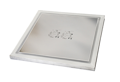
7. Frameless SMT Stencil - Foil/Plate Only (for universal frames)
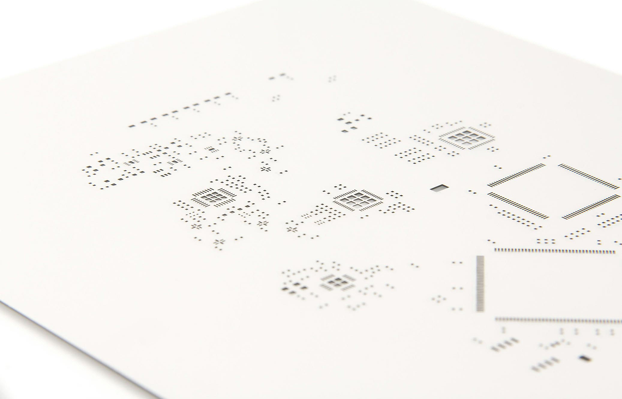
Foil or Plate Only stencils are designed to work within interchangeable plate or "universal" systems. Also referred to as "reusable", these stencils do not need to be permanently glued into a frame.
Frameless SMT Stencils also referred to as foils are laser cut solder paste stencils designed to work with stencil tensioning systems known as reusable stencil frames. This type of stencil does not need to be permanently glued in a frame. Frameless stencils are significantly less expensive than framed stencils and provide money-saving storage while still delivering superior quality and performance.
Frameless SMT Stencil Features:
- Reduced storage space requirements
- Significantly less expensive than framed stencils
- Excellent for prototype Printed Circuit Board Assembly or short runs
- Smooth aperture walls, can be used for 16 Mil pitch and below and for Micro BGA's
- 24-hour turnaround standard
| Frameless SMT Stencil Specs: | |
| Technology | 100% laser cut |
| Material Used | Stainless Steel |
| Stencil Thickness | 0.06 ~ 0.3 mm |
| Minimum Cut Width | 0.05 mm |
| Maximum Size | 280 X 380 mm |
| Allow for Fiducial Data | Yes |
| Allow for Panelized Data | Yes |
| Delivery | 1 ~2 Day |
8. Frameless SMT Stencil - Foil/Plate Only (for hand printing)
For times when you need precise control for smaller production runs, our Foil or Plate Only stencils are ideal. These frameless stencils allow you to hand print with precision just the amount you need and can be stored conveniently.
9. Electroformed SMT Stencils
Electroformed SMT stencils are nickel-based, electroform foils permanently mounted in a stencil frame using a mesh border to tightly stretch the stencil foil taut in the frame. Electroformed stencils offer the best paste release characteristics available and are frequently used for fine pitch (20 mil to 12 mil pitch) SMT applications on printed circuit boards. They are also used for µBGA's, Flip Chip, and Wafer Bumping (12 mil to 6 mil pitch).
Electroformed SMT Stencil Features:
- The smooth trapezoidal sidewalls of an electroformed stencil allow for better paste release
- Nickel has a lower coefficient of friction compared to stainless steel
- Electroform foils are harder than full hard stainless steel of comparable thickness, providing for longer stencil life
- 24-hour turnaround standard
| Electroformed SMT Stencil Specs: | |
| Technology | Electroforming |
| Material Used | Nickel |
| Suitable Applications | All Component Pitches |
| Aperture Tolerance | within 0.007mm |
| Stencil Thickness | 0.06 ~ 0.3 mm |
| 0.06mm.0.08mm.0.1mm.0.12mm.0.13mm.0.15mm.0.18mm.0.2mm.0.3mm | |
| Positional Accuracy | ± 0.008mm |
| Delivery | 1 ~2 Day |
What's the difference between a framed stencil and a frameless stencil?
A framed PCB stencil will have a 0.5" to 1.5" thick metal frame around it, similar to a picture frame. Framed stencils are often used by contract manufacturers, assembly and board houses, and large scale production facilities and are commonly placed in a manual or automated stencil printing machine. Frameless stencils are a thin sheet of material cut with a small border around your design. For example pictures on these products, please visit our Gallery.
What's the difference between Polyimide and Stainless Steel?
All stencils are made with high quality Polyimide and Stainless Steel. We use only the industry leading Stainless Steel, designed specifically for stencils. These materials are ideal for prototype or Multilayer PCB .
Stainless Steel: 0.0007" Laser spot size, 0.001" minimum aperature size.
Polyimide Film: 0.003" Laser spot size, 0.005" minimum aperature size.
Polyimide has a lower precision rate due to the way it is processed and its ability to withstand heat during the cutting process. Minor variances will occur when the material reacts to the laser. Paste release is great, but this material should be limited to a small number of uses and with components 0402 or bigger.
The minimum aperature size for Polyimide is 0.005" vs 0.001" for Stainless Steel. Polyimide also has a natural curl in the material caused by the way the film is manufacturered, this is outside of our control. Stainless Steel provides the ultimate in precision and quality, with a 0.0007" spot size, and exceptional paste release with a truly flat surface. If you want the absolute best reflow experience, there is no comparison, Stainless Steel is the superior material.
Analysis and Treatment of Common Problems in PCB SMT stencil
- Insufficient solder paste
- Smudging/bridging
- Misalignment print
- Bow and twist
How to Determine Stencil Size?
Stencil size is composed by two parts: internal size and overall size. Internal size is the size compatible with that of PCB ready to be assembled while overall size refers to the size compatible with printer parameter limit. As long as both sizes are accurately designed, stencil will be able to make full use of its functions.
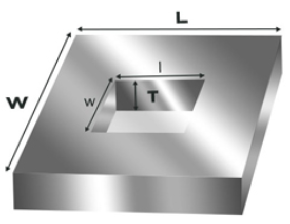
Internal size of stencil can be figured out conforming to the following rule:
- Width of Framed Stencil = width of PCB + 100mm while its Length = length of PCB + 100mm
- Width of Frameless stencil = width of PCB + 200mm while its Length = length of PCB + 200mm
For example, if one circuit board size is 50*50mm, then the size of its framed stencil should be around 150*150mm and the size of its frameless stencil should be around 250*250 mm.
It's easy to remember and operate so it worked for manual solder paste printing in SMT assembly prior to the advent of automatic printer. It can be said that different PCB sizes lead to generations of different internal sizes of stencil.
When it comes to automatic solder paste printer, however, it's relatively solid. Overall size of stencil has to be determined by parameter limit of the equipment, that is, printer, because stencil has to work within the range of printer with a frame. Different printers feature different parameter regulations. As far as PCBCart is concerned, the stencil size compatible with our printer can be either 650mm*650mm or 736mm*736mm.
PCB designers have to focus on internal size of stencil, they don't need to care about its overall size since it is generally determined by the parameters of printer in your contract assembler workshop.
How to Use PCB SMT Stencils?
PCB Stencil
PCB Stencil,SMT Stencil,SMD Stencil,Laser Stencil
JingHongYi PCB (HK) Co., Limited , https://www.pcbjhy.com
![<?echo $_SERVER['SERVER_NAME'];?>](/template/twentyseventeen/skin/images/header.jpg)