![<?echo $_SERVER['SERVER_NAME'];?>](/template/twentyseventeen/skin/images/header.jpg)
 The following is the circuit diagram of [CD4511 pin function circuit diagram]
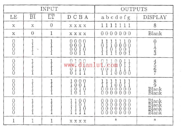
 The CD4511 is a set of packages used to decode the seven-segment display of a common cathode LED as a BCD. Its pin diagram, Figure 1 and the truth table shown in Figure 2, its pin functions are as follows:
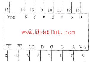
Figure 1 IC CD45111 pin function diagram
LT: For bulb test, when LT=0, the output abcdefg=1111111 regardless of other input states, so that the seven-segment display is fully illuminated, that is, display 8 to observe whether the seven-segment display is normal. When LT=1, it is normally decoded.
BI: blank input control, when BI=0 (LT is 1), regardless of the input of DCBA, its output abcdefg is 0, that is, the seven-segment display is completely off, this pin can be controlled by the user only for valid data translation. The code avoids the disorder of the font caused by the meaningless data input.
LE: Data latch enable control; in CD4511, not only has the function of decoding, but also has the memory function of data latching. When LE=0 (LT=1 and BI=1), the DCBA data will be sent to the IC's buffer for decoder code; when LE=1, the register in the IC will be turned off. Only DCBA data originally stored at LE=0 is saved for decoding by the decoder. In other words, when LE=1, regardless of the input data of the DCBA, the output is not affected, and the output abcdefg retains the data before the LE is changed from 0 to 1.
|
6.5Inch Coaxial Speaker,6.5 Inch Coaxial,6.5Inch Church Speaker,6.5 Inch Coaxial Speaker
Guangzhou BMY Electronic Limited company , https://www.bmy-speakers.com