![<?echo $_SERVER['SERVER_NAME'];?>](/template/twentyseventeen/skin/images/header.jpg)
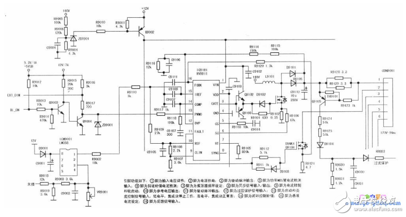
The following picture shows a group of LED backlight driving circuits in Changhong ITV46920DE LED LCD TV. Each group has the same circuit structure and is independent of each other. Each group of circuits drives an LED lamp group) application circuit. The LED driver circuit has an output voltage of 170V/90mA. Like the backlight driving circuit in the Hisense LED LCD TV seen earlier, the integrated block HV9911NCJ in the backlight driving circuit is also an LED backlight driving IC. The integrated block has a single switch drive mode controller, high-side current detection circuit, output current closed-loop control circuit, high PWM dimming ratio circuit, internal linear regulator from 9V to 250V, constant frequency or constant off-time control circuit. , VDD = 10V output short circuit protection circuit, output over voltage protection, synchronous lock circuit, programmable MOSFET current limit circuit, soft start and other module circuits.
The operation process of the LED backlight driving circuit in the following figure is: when the switching power supply is switched from the standby state to the normal working state, the 130V voltage of the power supply output is divided by the resistors R9006, R9005, and R9004, and a voltage of about 2.47V is formed on the R9004. Add to the gate of ZDT9001 and turn on ZDT9001. At this time, the voltage of 12V passes through R9011, R9010, and ZDT9001 to ground. After voltage division, a voltage of 11.25V is formed on R9010H. This voltage is applied to the base of Q9002 to make the Q9002 saturate and turn on. At this time, the voltage of 12V passes through the Q9002e-c pole. It is output from the c-pole to the 1st pin of HV9911NG (Note: It is also applied to the 1st pin of IC9201, IC9301, IC9401, IC9501, and IC9601) as the operating voltage of HV9911NG (IC9201, IC9301, IC9401, IC9501, IC9601).
At the same time, the start control voltage "BL_ON" (high level) of the backlight driving circuit output on the signal processing board is divided by the resistor R9013 and the resistor R9003 to form a voltage of 0.56V applied to the base of the Q9003, so that the Q9003 is satisfactorily turned on. . The collector voltage changes from high level to low level. At this time, Q9004 enters the off state due to the absence of voltage at the base. The +5VS voltage is applied to the 13 pins of the IC9101 via R9016 and R9017. To the IC9201, IC9301, IC9401, IC9501, and 13960 of IC9601). After the pins 1 and 13 of the integrated block IC9101 are powered, the internal oscillating circuit will start to enter the working state, generating an oscillating pulse signal. The oscillating pulse signal generated by the oscillating circuit is processed by the internal correlation circuit, and is output from the pin of the integrated block 3, and directly applied to the base of the Q9102 and Q9103 as its input signal.
The reference voltage (1, 24V) formed by the HV9911NG internal reference voltage generation circuit is output from pin 10. This reference voltage is applied to the HV9911NG(15) pin via resistor R9107 as the reference voltage for the pin.
The external resistor R9105 of the HV9911NG7 pin is a frequency setting resistor. By changing the size of the resistor, the frequency of the oscillator can be adjusted. Once the resistance of the resistor R9105 is determined, the oscillation frequency of the oscillator is determined. Thereafter, the oscillator will operate at the set natural oscillation frequency.
The driving pulse signal outputted by the HV9911NG3 pin is amplified by Q9012, and then applied to the gate of Q9101 via the resistor R9101, so that the Q9101 operates in the switching state.
After the Q9101 is turned on, the current forms a loop through the "D" pole of the 130V→L9101→Q9101→the “S†pole of the Q9101→R9102→, and the energy is stored in the L9101, generating a left positive and a negative voltage. After the Q9101 is turned off, since the current at both ends of the inductor cannot be abruptly changed, a left negative right positive voltage is formed across the L9101. The voltage is charged to the capacitor C9110 via D9101 and D9105, so that the voltage of 130V+L901 is charged to the C9110, After the voltage superposition result is obtained as a DC voltage of 170V/90mA, it is applied to the LED light-emitting diode (light bar) via the resistors R9128 and R9129 as the driving voltage for lighting the LED strip.
In the circuit, the circuit composed of Q9103 and D9102 is a perfusion circuit. The function of the circuit is the same as the perfusion circuit in the driving circuit of the Hisense LED LCD TV backlight lamp introduced above, in order to bleed between the gate and the source during the Q9101 off period. Designed for stored charge.
The working process of the perfusion circuit is: when the 3 pin of the HV9911NG outputs a low level, the Q9102 is turned off, and the Q9103 is turned on. After the Q9102 is turned off, the source voltage is low, and the Q9101 turns from on to off. At this time, since Q9103 is turned on, the charge accumulated on the gate of Q9101 is discharged through the D9102→Q9102 source→Q9102 drain, thereby effectively preventing the Q9101 from being damaged due to charge accumulation between the gate and the source.
In order to make the abnormality of the switch tube in the bootstrap boost circuit without expanding the fault range, a current feedback circuit composed of internal circuits of the R9602, R9603 and HV9911NG5 pins is also designed in the circuit. R9602 in the circuit is the sampling resistor, and pin 5 is the current feedback detection signal input terminal. The current feedback circuit is realized by current detection of the switching transistor Q9101. When the switching transistor Q9101 works abnormally, the current flowing through the drain-source increases, the voltage drop across the resistor R9102 increases, and the increased voltage is applied to the HV99115 pin via R9103, after entering the internal circuit of the integrated block, internally The relevant circuit performs processing, and the processing ends the output control signal to the driving pulse output circuit to stop the operation without the pulse signal output, thereby implementing the overcurrent protection of the switching tube.
Changhong ITV46920DE LED LCD TV backlight driver is designed with brightness setting circuit. The circuit consists of R9018, R9019, R9003, VR9001 and ICM9001.
In the figure below, the 12V voltage is divided by a series circuit composed of resistors R9018 and R9019 to obtain a voltage of about 3.58V on R9019. The voltage is divided by resistor R9003 and potentiometer VR9001 and added to the 3rd pin of the integrated block ICM9001. The pin is the positive input of the internal comparator.
ICM9001's 1 pin via resistor R9002 is connected to pin 15 of HV9911NG. HV9911NG (15) pin is the current setting terminal of the drive pulse forming circuit. When the potentiometer VR9001 is changed to the 3 pin potential of ICM9001, the 1 pin voltage will occur. Change, 1 pin voltage change is also the HV9911NG (15) pin output current setting changes, (15) foot set current change will inevitably change the width of the output pulse of the drive pulse forming circuit, and finally achieve the purpose of adjusting the backlight brightness according to design requirements .
The current stabilizing circuit in the backlight driving circuit is composed of Q9104, R9121 and internal related circuits of the integrated block HV9911NG (16) pin.
When the current flowing through the LED strip increases or decreases, the current flowing through Q9104 and R9121 also increases or decreases, and the voltage drop formed by the varying current on R9121 also increases or decreases. The voltage formed on R9121 reflecting the current of the LED strip is applied to the (16) pin of HV9911NG via R9120. After being processed by the internal circuit of HV9911NG, the control signal is output to control the duty cycle of the driving pulse of the integrated block 3 pin. The adjustment of the pulse duty cycle returns the LED strip current to a normal value, thereby achieving stable LED strip current.
The protection circuit in the backlight driving circuit is divided into overvoltage and overcurrent protection.
The overvoltage protection circuit is mainly composed of R9114, R9115, R9116 and internal related circuits of the integrated block HV9911NG(12). When the output voltage of the LED driver circuit rises abnormally for some reason, the boosted voltage is divided by the series circuit composed of R9114, R9115, and R9116, and then added to the integrated block HV9911NG(12) pin, (12) pin input. After the voltage is processed by a protection circuit such as a voltage comparator inside the integrated block, the control signal is output to the drive pulse output circuit to stop the operation without the drive pulse output.
The overcurrent protection circuit is protected by stopping the main power supply, and is composed of R9128, R9129, R9123, R9124, R9125, Q9105, and D9104. The overcurrent protection circuit is for the short circuit protection of the LEDs inside the LED strip.
When the TV is normal, the current flowing through the resistors R9128 and R9129 is small, and the voltage drop across it is also low. The base voltage of Q9105 is substantially equal to the emitter voltage, and Q9105 is turned off, which is equivalent to the overcurrent protection circuit stopping. When the LED on the internal LED strip of the screen has a severe breakdown short circuit fault, the LED strip current will increase sharply. At this time, the base voltage of Q9105 will drop sharply, turning Q9105 from off to on. The 170V output from the driver circuit is added to the QB857 via the emitter, collector, R9124, R9125, D9104, DB9006, and RB883 of Q9105. The base pole makes the QB857 saturate and conducts, the optocoupler PCB803S in the main power supply enters the working state, the secondary output overcurrent detection signal is sent to the 10th pin of the integrated block IC801 in the main power supply, and the signal input by the 10 pin is integrated into the internal circuit of the integrated block. After processing, the control signal is output to stop the main power supply in the switching power supply.
Door Bell Switch,Doorbell Switch,Doorbell Switch With Light,Doorbell Button Cover Plate
ZHEJIANG HUAYAN ELECTRIC CO.,LTD , https://www.huayanelectric.com