![<?echo $_SERVER['SERVER_NAME'];?>](/template/twentyseventeen/skin/images/header.jpg)
Whether it's discrete logic, programmable logic, or any digital design implemented using fully custom silicon devices, a stable and reliable clock signal is essential for proper functionality. Poorly designed clocks can lead to unpredictable behavior under extreme temperature, voltage, or manufacturing process variations, making them difficult to debug and potentially costly to fix. When designing a PLD/FPGA, several types of clock signals are commonly used. These include global clocks, gated clocks, multi-level logic clocks, and wave clocks. A multi-clock system may combine any of these four types.
1. Global ClockThe global clock, also known as the synchronous clock, is the simplest and most predictable type of clock in a PLD/FPGA design. The ideal clocking scheme involves using a single master clock that drives all flip-flops in the design through a dedicated global clock input pin. Whenever possible, designers should prioritize using a global clock due to its reliability and minimal delay. Most PLDs and FPGAs feature a dedicated global clock pin that connects directly to each register in the device, ensuring the shortest clock-to-output delay.
Figure 1 illustrates an example of a global clock. The timing waveform shows that the data inputs D[1..3] of the flip-flop must meet setup and hold time requirements. These values are typically specified in the PLD data sheet and can be verified using the software’s timing analyzer. If these timing constraints are not met, the input signal must be synchronized (as discussed in the next chapter on "Asynchronous Inputs").
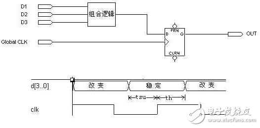
Figure 1: Global Clock
(The best approach is to use the global clock pin to drive every register in the PLD, so the data only needs to meet the relative clock setup time tsu and hold time th.)
2. Gated ClockIn many applications, it may not be feasible or practical to use a global clock for the entire design. PLDs often provide a product term logic array clock, which allows certain functions to generate individual clock signals for specific flip-flops. However, when using such a clock, it's crucial to carefully analyze the logic to avoid potential glitches.
Gated clocks are typically created using this logic-based approach. They are often found in microprocessor interfaces, where address lines control write pulses. Any clock that is triggered by a combination of logic signals is essentially a gated clock. A gated clock can function reliably if the following conditions are met:
- The logic driving the clock should contain only one AND gate or one OR gate. Adding more complex logic may introduce glitches due to race conditions.
- One input to the logic gate acts as the actual clock, while other inputs should be treated as addresses or control signals that follow strict setup and hold time constraints.
Figures 2 and 3 show examples of reliable gated clocks. In Figure 2, an AND gate is used to generate the gated clock, while Figure 3 uses an OR gate. In both cases, the pins nWR and nWE are considered clock pins, while the address lines ADD[0..3] act as control signals. The data for the two flip-flops is generated by random logic from the signal D[1..n].
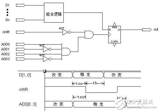
Figure 2: AND Gated Clock
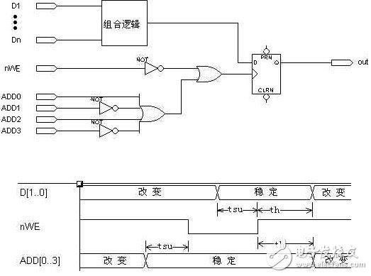
Figure 3: OR Gated Clock
The waveforms in Figures 2 and 3 demonstrate the setup and hold time requirements. The address lines must remain stable throughout the period when the clock is active (nWR and nWE are active low). If the address lines change during this time, a glitch may occur on the clock line, leading to incorrect state transitions in the flip-flop. On the other hand, the data pins D[1..n] only need to meet standard setup and hold times at the valid edges of nWR and nWE.
Designers can often convert a gated clock into a global clock to improve reliability. Figure 4 shows how the circuit from Figure 2 can be redesigned with a global clock. Instead of using the address line to generate the clock, it is used to control the enable input of a D flip-flop. Many PLD design tools, such as MAX+PLUSII, support this configuration. When ENA is high, the D input is latched; when ENA is low, the current state is retained.
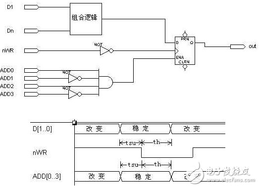
Figure 4: AND Gated Clock Converted to Global Clock
The timing waveform of the redesigned circuit in Figure 4 indicates that the address lines no longer need to be stable for the entire duration of nWR. Instead, they only need to meet the same setup and hold time requirements as the data pins, reducing the complexity of the design.
Figure 5 shows an example of an unreliable gated clock. The RCO output of a 3-bit synchronous counter is used to clock a flip-flop. However, since multiple inputs from the counter are used as the clock, it violates the conditions required for a reliable gated clock. None of the flip-flops generating the RCO signal can be considered true clock lines because they all toggle almost simultaneously. But since the routing paths for QA, QB, and QC to the D flip-flop may vary in length, a glitch can appear on the RCO line, as shown in the timing waveform of Figure 5. For instance, if the path from QC to the D flip-flop is shorter, its output will toggle first, causing instability.
SVLEC provide M8 M12 junction box, which connects Sensors and actuators to the control system. They are ideal for harsh conditions, especially for cooling and lubricants. Fully encapsulated housing provides a higher level of protection and excellent shock and vibration resistance .


Distribution System,M8 Junction Box,M23 Input Distribution Box,Distribution Box with PCB plug,M12 Distribution System
Kunshan SVL Electric Co.,Ltd , https://www.svlelectric.com