![<?echo $_SERVER['SERVER_NAME'];?>](/template/twentyseventeen/skin/images/header.jpg)
(1) Notes on using TTL integrated circuits
The power supply voltage of the 1TTL integrated circuit cannot be higher than +5.5V. The power supply and the ground cannot be connected in reverse. Otherwise, the device will be damaged due to excessive current.
The input terminals of the 2 circuit cannot be directly connected to the low internal resistance power supply higher than +5.5V and lower than -0.5V, because the low internal resistance power supply can supply a large current, causing the device to overheat and burn out.
3 Except for the three-state and open-collector circuits, the output terminals are not allowed to be used in parallel. If the gate output of the T306 dual-in-line open collector is used in parallel to make the circuit have line and function, a pre-calculated pull-up load resistor should be added to the VCC terminal at its output.
4 output does not allow short circuit with power or ground. Failure to do so may result in damage to the device. However, it can be connected to ground through a resistor to increase the output level.
5 Do not move or insert the integrated circuit while the power is on, as the impact of the current may cause permanent damage.
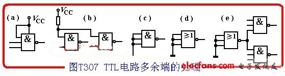
6 The extra input should not be left floating. Although the dangling is equivalent to a high level, it does not affect the logic function of the NAND gate, but the dangling is easily disturbed, sometimes causing malfunction of the circuit, and the performance is more obvious in the sequential circuit. Therefore, the redundant input is generally not suspended, but processed as needed. For example, the redundant inputs of the AND gate and the NAND gate can be directly connected to the VCC; different inputs can be connected to the VCC through a common resistor (several thousand ohms); or the redundant input and the terminal can be connected in parallel. . All inputs to unused devices such as gates and NAND gates can be grounded, or their outputs can be connected to unused AND gate inputs. As shown in Figure T307.
For triggers, the unused input cannot be left floating and should be connected to the level according to the logic function. The input wiring should be as short as possible to shorten the delay time of the clock signal along the transmission line in the sequential circuit. It is generally not allowed to directly drive the output of the trigger to the indicator light, inductive load, long-line transmission, and a buffer door must be added when needed.
Magnetic Switch,Magnetic Reed Switch,Magnetic Door Switch,Magnetic Contact Switch
NINGBO SANCO ELECTRONICS CO., LTD. , https://www.sancobuzzer.com