![<?echo $_SERVER['SERVER_NAME'];?>](/template/twentyseventeen/skin/images/header.jpg)
Serial interconnection forms the key foundation of modern communication systems , so the choice of serializer / deserializer (SerDes) can have a large impact on system cost and performance. Although traditional data-based communication The SerDes cater for the appropriate byte (byte-oriented) oriented, packet-based (packet-based) design of the bus, but many other telecommunication applications bus format. This makes it very difficult to design SerDes technology into these systems. This article summarizes the SerDes architecture, and displays a description of how a particular architecture suitable for telecommunications signal processing system.
SerDes architecture: an overviewThe parallel clock SerDes serializes the parallel wide bus into multiple differential signal pairs and transmits the clock in parallel with the data. These SerDes are relatively inexpensive, and can effectively expand a wide bus through cables or backplanes in applications where multiple SerDes are commonly required .
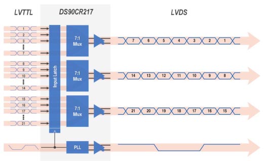
Figure 1. DS90CR217 21 -bit channel-link parallel clock serializer
Input latch | Input latch |
Mux | Multiplexer |
8b / 10b SerDes maps each data byte to a 10 -bit code and then serializes it into a single signal pair. The 10 -bit code is defined as follows: to provide sufficient conversion for receiver clock recovery and to ensure DC balance (send equal numbers of "1" and "0") These attributes enable 8b / 10b SerDes to operate at high speeds with less signal distortion on lossy interconnects and fiber optic cables.
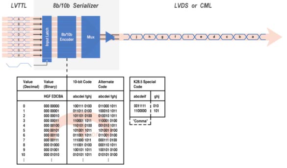
Figure 2. 8b / 10b serializer block diagram
8b / 10b serializer | 8b / 10b serializer |
LVDS or CML | LVDS or CML |
Input latch | Input latch |
8b / 10b encoder | 8b / 10b encoder |
Mux | Multiplexer |
Value (decimal) | Value ( decimal ) |
Value (binary) | Value ( binary ) |
10-bit code | 10 -digit code |
Alternate code | Optional code |
K28.5 special code | K28.5 special code |
Comma | comma |
Bit-interleaved SerDes aggregates bits from multiple input serial streams into a faster serial signal pair. This type of SerDes maximizes throughput with minimal wiring.
Â
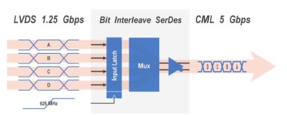
Figure 3. Block diagram of a bit interleaved serializer.
Bit interleave SerDes | Bit interleaved SerDes |
Input latch | Input latch |
Mux | Multiplexer |
Â
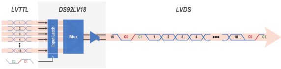
Figure 4. The DS92LV18 18 -bit bus LVDS embedded clock is a serializer
Input latch | Input latch |
Mux | Multiplexer |
The embedded clock bit architecture can serialize the data bus and clock into a serial signal pair. Two clock bits, one low and one high, embed a serial data stream in each clock cycle, framing the beginning and end of each serialized word (hence the name of the optional alternative is Start - stop bit " SerDes ), and create a periodic rising edge in the serial stream. Since the payload is sandwiched between embedded clock bits, the data payload word width is not limited to multiples of bytes. In fact, 10 and 18 -bit bus products are available. Â
Â
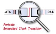
Figure 5. Periodic embedded clock bit conversion.
Period embedded clock transiTIon | Periodic embedded clock bit conversion |
After power-up, the receiver automatically searches for the rising edge of the regular embedded clock. Because the data bits of the data payload change value over time, but the clock bits do not change over time, the receiver can locate and synchronize with unique clock edges. After locking, the receiver recovers data from the serial stream regardless of the payload data pattern. This automatic synchronization function is often referred to as "locking to random data" and requires no external system intervention. This is a particularly useful function in systems where the receiver is located in a remote module that is not directly controlled by the system, and in systems where one transmitter broadcasts to multiple receivers. In the case of broadcasting, the new receiver module plugged into the bus will lock to random data without the need to interrupt communication to other receivers by sending training patterns or characters.
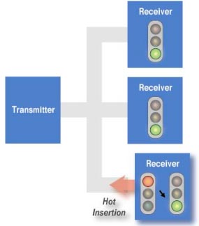
Figure 6. The receiver automatically locks to random data during hot insertion.
Transmitter | Transmitter |
Receiver | receiver |
Hot inserTIon | Hot insertion |
Most SerDes rely on strict control of the jitter of the sending and receiving clocks to achieve lock and lock monitoring. However, the embedded clock bit receiver synchronizes the rising edge of the input embedded clock and requires the receiver reference clock only during the initial synchronization to prevent locking to false harmonics. This can relax the jitter requirements of the transmit and reference clocks by at least an order of magnitude. In fact, the receiver reference clock only needs to be Within ± 50,000 PPM . This can save a lot of cost in a system that uses a non-standard oscillator, because standard frequencies with very low cost can be used.
System comparisonThe embedded clock bit SerDes is particularly suitable for applications that send raw data and other signals such as control, parity, frame, status, etc. For example, signal processing systems for base stations, car imaging / video and sensors, where analog / digital converters, cameras or displays pass raw data to the signal processing unit at the other end of the link. For the purpose of explanation, it is assumed that DS92LV18 of National Semiconductor is used in the data acquisition system of FIG. 7 . Here DS92LV18 not only serializes the data, but also serializes two bits of additional information, such as parity, status bits, etc. These bits are serialized together with the data bits at the normal A / D sampling rate, so that there is no need to use data buffers or additional logic circuits.
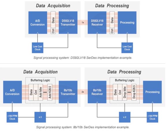
Figure 7. Example implementation of a signal processing system based on DS92LV18 SerDes ( above ) and 8b / 10b SerDes ( below ) .
Data acquisiTIon | data collection |
A / D conversion | A / D conversion |
Data | data |
Ctrl | control |
Transmitter | Transmitter |
Low cost clock | Low cost clock |
Data processing | data processing |
processing | deal with |
Signal processing system: DS92LV18 SerDes implemenTIon example. | Signal processing system : DS92LV18 SerDes implementation example. |
Buffering logic | Buffer logic |
Add idle | Add Idle |
|
A DC motor is any of a class of rotary electrical machines that converts direct current electrical energy into mechanical energy. The most common types rely on the forces produced by magnetic fields. Nearly all types of DC motors have some internal mechanism, either electromechanical or electronic, to periodically change the direction of current flow in part of the motor.
DC motors were the first form of motor widely used, as they could be powered from existing direct-current lighting power distribution systems. A DC motor's speed can be controlled over a wide range, using either a variable supply voltage or by changing the strength of current in its field windings. Small DC motors are used in tools, toys, and appliances. The universal motor can operate on direct current but is a lightweight brushed motor used for portable power tools and appliances. Larger DC motors are currently used in propulsion of electric vehicles, elevator and hoists, and in drives for steel rolling mills. The advent of power electronics has made replacement of DC motors with AC motors possible in many applications. DC Gear Motor,DC Shunt Motor,Shunt Motor,Small DC Motor Shenzhen Maintex Intelligent Control Co., Ltd. , https://www.maintexmotor.com |