![<?echo $_SERVER['SERVER_NAME'];?>](/template/twentyseventeen/skin/images/header.jpg)
AZZURRO from Germany was established in 2003, mainly to provide new-type wafers for power semiconductor and LED manufacturers. AZZURRO has an exclusive patented GaN-on-Si technology. Their method is to first grow a buffer layer based on GaN material on the silicon substrate, and then depending on the LED or power Different applications in the semiconductor industry generate GaN films on this wafer. The company pointed out that it is now possible to produce GaN on Si wafers on 6-inch (150mm) silicon substrates, and even challenges 8-inch (200 mm). LEDinside expects this new process to effectively solve existing LED production equipment Difficulties in transferring LED process to silicon substrate. LEDinside had the privilege of interviewing Mr. Erwin Ysewijn, vice president of AZZURRO's marketing business, to share AZZURRO's technology and experience.
Mr. Erwin Ysewijn, VP Sales & Market of AZZURRO
GaN-on-Si technology difficulties and cost savings
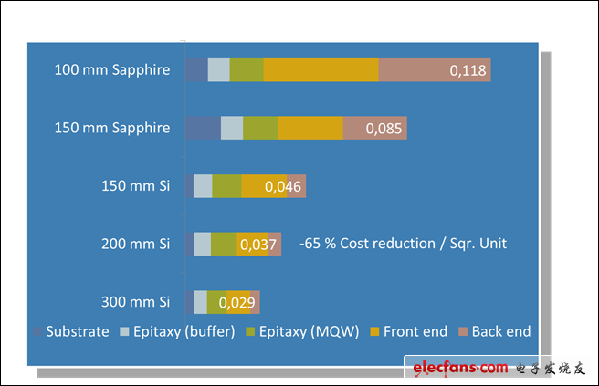
GaN-on-Si can be said to be a hot topic in the LED industry recently, and its maturity has been improving. It is one of the technologies for future development. However, LEDinside analysis, due to the current technical difficulties focus on the thermal expansion coefficient of the material and the lattice misalignment, because the thermal expansion coefficient of the silicon substrate and GaN are different, the process will cause stress due to the lattice misalignment between the two materials, Furthermore, the problems of bow, crack and uneven film thickness are formed. There are certain difficulties to overcome these problems. It is not a general LED manufacturer that can complete it independently. It has not been widely used in the LED industry in the past, but if it can overcome the above problems and successfully generate a Gan layer LED wafer on a silicon substrate ( Epitaxial wafer), which can benefit from the good conductivity of the silicon substrate. The LEDs created at that time will generate less heat energy, which will help simplify the heat dissipation design of LED application products. LEDinside believes that this move can improve the wavelength uniformity and thickness uniformity of LED wafers, make the wavelength more concentrated, greatly reduce the cost of post-stage inspection of epitaxy plants, and greatly improve the yield. According to AZZURRO, if we compare the LEDs generated by a 6-inch Gan-on Si substrate with a sapphire substrate, the recent mature technology estimates that the cost of the former can be reduced by up to 75%.
According to the GaN on Si wafer data released by AZZURRO, the standard deviation of the curvature is reduced to only 0.764% for 150mm (6 inch) wafers, which is almost 1.0% compared to the 4-inch sapphire substrate. The performance is more outstanding, and there is a chance to improve further. Compared with sapphire substrates, the use of silicon substrates, in addition to cost advantages, LED manufacturers can use the existing silicon wafer process technology, after cutting and other post-process technologies can be supported.
In addition, when producing flip chip LEDs, the silicon crystal material is easier to remove than sapphire. The production cycle can not only be significantly shortened, but also a better yield can be obtained. In order to save cost and production time, LED manufacturers switch to using large-sized substrates, and silicon substrates have a very good advantage.
GaN-on-Si market development
AZZURRO is optimistic that Taiwan has a complete LED industry supply chain, and pays special attention to it. It not only establishes a technology and customer service team in Taiwan, but also assists customers in process conversion. AZZURRO said that when customers adopt the GaN on Si process, AZZURRO will support customers to complete the epitaxial growth stage, and it is estimated that customers will only need 8 to 16 weeks for the later stage of the chip process.
Editorial point of view
Observing the development of the GaN-on-Si market in 2012, currently limited by the large-size sapphire substrate production and technology is difficult to develop, the price of sapphire substrates above 6 inches is also high, most LED manufacturers still use 2 inch and 4 inch substrates. However, at present, all front-line LED epitaxial manufacturers around the world are conducting GaN on Si wafer experimentation. In addition, European and American manufacturers also accelerated the establishment of 6-inch GaN on Si wafer production lines in 2012. After the mass production phase is completed, the cost performance and luminous efficiency can achieve a win-win situation.
LEDinside believes that the rapid introduction of this new technology is a new method for the LED industry to reduce costs and increase production capacity. At the same time, existing production equipment has the opportunity to add value and switch to a new process. In the long run, overall output and unit cost will continue to go down, and whether and when the market's application demand can increase significantly is believed to be the most important issue in the future.
AS cylindrical rechargeable Lithium Ion Battery, 18650 Cell size is high 65mm and diameter 18mm. Nominal Votage: 3.7V, max Voltage:4.2V, Maximum charge current: 1C, Max discharge current: 1.5C. It can be used for electronic products, such as lighting equipment, medical devices,power bank and so on.
18650 Battery Cell,Li-Po Battery Cell 3.7V,18650 Lithium Battery,Battery 18650
Shenzhen Powercom Electronics Co., Ltd. , https://www.expowercome.com