![<?echo $_SERVER['SERVER_NAME'];?>](/template/twentyseventeen/skin/images/header.jpg)
Abstract: ApplicaTIon Note 354 provides a logical diagram of the clock map of the Dallas Semiconductor / Maxim DS2154 and DS2152 single chip transceivers (SCTs).
Figure 1 logically describes the clock map of the DS2152 and DS2154 Single Chip Transceivers. Although there is only one Jitter Attenuator, which can be placed in the receive or transmit path, two are shown for simplificaTIon and clarity.
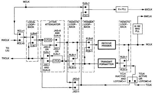
Figure 1. Clock map.
NotesThe PAYLOAD loopback switch is not included on the DS2154
.
Figure 1 logically describes the clock map of the DS2152 and DS2154 Single Chip Transceivers. Although there is only one Jitter Attenuator, which can be placed in the receive or transmit path, two are shown for simplificaTIon and clarity.
Figure 1. Clock map.
NotesThe PAYLOAD loopback switch is not included on the DS2154
.
| LTCA = Long Term Clock Average | ||
| RLB = Remote LoopBack | JAS = Jitter Attenuator Select | |
| FLB = Framer LoopBack | DJA = Disable Jitter Attenuator | |
| PLB = Payload LoopBack | RCL = Receive Carrier Loss | |
| LLB = Local Loopback | LOTCMC = Loss Of Transmit Clock Mux Control | |
| RXCLK = Recovered clock from LIU | ||
| TXCLK = Transmit rate clock for LIU | ||
Solar System Batteries,60Ah Ni-Fe Battery,24V Nickel Iron Battery Bank 60Ah,Ni-Fe Battery 10~80Ah
Henan Xintaihang Power Source Co.,Ltd , https://www.taihangbattery.com