![<?echo $_SERVER['SERVER_NAME'];?>](/template/twentyseventeen/skin/images/header.jpg)
The simplest technique for measuring current in an actuator or motor is to monitor its ground current by sensing the voltage drop across a small resisTIve element, added between the load and ground. Because the device and its associated electronics share the same ground potenTIal, you need only amplify the ground-current signal.
That approach, however, does not detect device shorts to ground, which can overload the high-side drive circuitry. To mitigate such potential fault conditions, a high-side current monitor will detect short circuits and similar faults downstream from the current monitor.
High-side current monitoring has advantages, but its use has been limited by a shortage of devices able to handle the high voltage levels used in industry (from 24V to many 100s of volts). Off-the-shelf devices can operate to 32V and to 76VDC, but even 76VDC is not enough for many applications. Figure 1 shows a simple way to adapt a standard 32V device for use at any voltage level, subject to limitations in the external components. (The components shown support 130V.) Accuracy is better than 1% for load currents greater than 30mA.
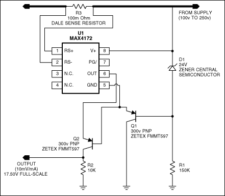
Figure 1. The components shown enable a 36V high-side current-monitoring IC (U1) to operate at common-mode voltages as high as 130V. (For higher voltages, re-size R1 as suggested in the text.)
U1 was selected for its current-output stage, which allows easy implementation of the current mirror necessary for level-shifting the output signal to ground. Then, the ground-referenced signal is easily monitored with an A / D converter or comparator.
In this application, current applied to the load is monitored in the presence of a 130VDC common-mode level. First, ensure that U1's absolute maximum rating (36VDC with respect to the GND pin) is not violated for the Rs +, Rs-, and V + pins. For that purpose, the 24V zener diode Z1 limits voltages between the V +, Rs +, and GND pins to 24V. Thus, the typical voltage between these pins is 24V minus the Vbe of Q1, or 23.3V.
Izener for this circuit is approximately 700µA. Note: the manufacturer's suggested bias current is 500µA, but the zener's di / dt slope goes negative below 300µA, which can introduce noise and even oscillation (Figure 2). The minimum specified bias (300µA to 500µA ) sets the maximum value of R1, and the maximum allowed power dissipation for R1 and D1 combined sets the minimum value for R1. Thus, for supply rails between 100V and 250V a reasonable R1 value is between 150k and 225k
(150k
in this case).
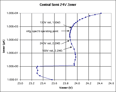
Figure 2. This graph of Vzener vs. Izener (for the zener diode in Figure 1) indicates Izener values ​​corresponding to various combinations of high-side voltage and R1. For bias currents below ~ 400mA, note that the slope of this curve (indicating the zener's dynamic source impedance) goes negative, producing additional noise and the possibility of oscillation.
Q1 and R1 form a shunt regulator. Q1 was selected for its maximum VCE rating (-300V), its high gain (100V / V at 1.0mA), and its power-handling capability (500mW). Output current is proportional to the voltage difference (Vsense) between Rs + and Rs-: Iout = Gm x Vsense, where Vsense = Rsense x Iload. Gm for U1 is 10mA / V. If the maximum monitored load current (Iload) is 4A, and Rsense = 10m , the maximum Iout is 10mA / V x 10m
x 4A = 400uA.
Thus, Iout is proportional to Iload, and the maximum expected output is 400uA. For applications of wide dynamic range in which Vsense can approach the absolute-maximum rating of the internal differential pair (700mV), you should protect the sense pins by adding series resistors between Rsense and Rs +, and between Rsense and Rs-. The resistor values ​​should be selected to limit input currents to <10mA when the Rs + to Rs- difference is 700mV.
Iout is now proportional to Iload, but for easy monitoring it must be level shifted to ground by the current mirror consisting of Q2 and R2. Q2's high gain forces the collector current to closely approximate the emitter current, which, applied to R2, produces a voltage that can be measured at Vout. Like Q1, Q2 needs a maximum Vce rating of -240V minimum (the device shown is rated -300V).
Vout now equals Iout x R2 (the actual output current at Q2's collector is slightly less, due to the outflow of Q2 base current.) At Iload = 4A, Vout = 400uA x 10.0K = 4.0V. Designs with lower or higher operating voltage can be accommodated by proper selection of Q1, Q2, and the base resistor R1.
This design idea appeared in the July 22, 2004 issue of EDN magazine.
TM1914 Digital LED Strip is a double signal transmission led strip,mainly use in 5050RGBWW 5in 1 led strip,the TM1914IC is outside on the strip,
To achieve the Digital and dimmer color by a extend controller . More functions can to change the range of digital color,
the Color Temperature is range of the 2600-6500K. Meet the needs of different scenarios.
TM1914 Digital LED Strip
Rgbw Led,Tm1914 White LED Strip Light,TM1914 LED Strip,TM1914 Digital LED Strip
SHEN ZHEN SEL LIGHTING CO.,LTD , https://www.sel-lighting.com