![<?echo $_SERVER['SERVER_NAME'];?>](/template/twentyseventeen/skin/images/header.jpg)
Tuning the MAX2009 / MAX2010 RF Predistorters for OpTImal Performance
Abstract: Linear modulaTIon schemes like WCDMA allow higher data rates and mulTIple wireless connecTIons per carrier, but introduce a high peak-to-average ratio of the carrier signals. Consequently, the amplifier now has to be largely backed off to meet the limits for adjacent -channel leakage. Since the PA's (power amplifier's) efficiency decreases the more the PA is backed off, linearization techniques are applied to combine a maximum efficiency with a minimum of IM (intermodulation). This application note details different techniques for tuning the MAX2009 / MAX2010 analog predistorters while optimizing the ICs' performance.
Well-known linearization technologies, eg, feed forward (FFW) and digital predistortion (DPD) are expensive and need considerable space. Consequently, a method is needed that works with few components and is easy to handle.
The MAX2009 / MAX2010 analog RF predistorters, when compared to FFW or DPD, need very few external components, are easy to adjust, and give a considerable amount of linearization.
The MAX2009 / MAX2010 rely on AM-AM and AM-PM curve correction at the RF frequencies to improve IM3 and ACPR performance. Internally, the chip measures the signal power and distorts the phase and gain predistortion as a function of the current signal's amplitude. Although AM-AM and AM-PM correction rely on memory-less circuits, Class AB amplifiers can still benefit from the negative distortion created by the Maxim® parts and significantly improve performance.
As with all linearization techniques, a good signal-clipping algorithm which reduces the peak-to-average ratio of the signals before the PA (without exceeding the EMV limits) is helpful for analog predistortion. Using the MAX2009 / MAX2010 together with proper signal clipping is a good combination.
General Predistorter TheoryGiven a sinusoidal RF input signal, the amplifier compression distortion at the RF frequencies typically looks like Figure 1. The predistorter distorts the input signal to counter the distortion added by the amplifier. The result is a net linear transfer function.
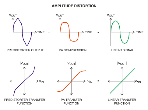
Figure 1. Amplitude-distortion transfer functions.
Phase distortion works in much the same way. Most amplifiers tend to delay the input signal more with an increase in amplitude. This means that the output signal's phase decrease with an amplitude increase. The predistorter's phase section does the opposite by reducing the delay as a function of amplitude. The net result is a constant delay transfer function.
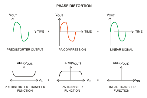
Figure 2. Phase-distortion transfer functions.
The previous figures showed the instantaneous VIN / VOUT characteristics. This is difficult, if not impossible, to obtain for an RF amplifier. One can fully characterize the nonlinear behavior of the amplifier by simply plotting the AM-AM and AM-PM plots, given a memory-less system. An example of AM-AM and AM-PM plots is shown in Figure 3. The input signal is a single frequency; the x-axis is the input power; and the AM-AM and AM-PM plots show the magnitude and phase of the gain, respectively. Note that the phase compression begins before the amplitude compression takes place. This is important for choosing the proper analog predistortion method.
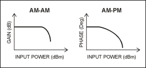
Figure 3. AM-AM and AM-PM plots.
Every practically realizable amplifier shows some amount of nonlinearity, which can be described by a nonlinear transfer function represented by a Taylor expansion: VOUT = K0 + K1VIN + K2VIN² + K3VIN³ + ... + KNVINN The even constants produce harmonics that are far away from the fundamental and are, therefore, insignificant. Furthermore, the magnitude of the products decreases with higher order. Therefore, in most cases practical nonlinear amplifiers can be described to a sufficient accuracy using third- and fifth-order products only. Depending on the amount of required linearization, higher-order products can become important in some cases. The higher K3, K5 ... become, the more nonlinear is the amplifier. This results in AM-AM and AM-PM curves that deviate more and more from an ideal straight line. The goal for any kind of amplifier predistortion is to improve the system's AM-AM and AM-PM behavior as much as possible, thus minimizing unwanted intermodulation products.
How to Prepare an Amplifier for PredistortionThe general function of the MAX2009 / MAX2010 is to expand phase and gain to compensate the phase and gain compression of the amplifier. This process corresponds to a linear mapping, where every single point of the compression curve of the power transistor is given a single value of phase and gain correction. In reality, amplifiers suffer from memory effects to some extent. As with every semiconductor component, the properties of the power transistor vary over temperature. Because of the limited efficiency of power amplifiers, most of the power will be transferred into heat. This takes place with several different time constants. To heat up the whole amplifier can take minutes; to heat up the transistor package can take seconds, but the time constant for heating the channel of an LDMOS is in the range of microseconds.¹ So if the envelope power of a signal varies very quickly, eg, as with WCDMA, the temperature of the active channel will not r emain constant but change with the modulation. This causes memory effects. Restated simply, the amplifier behaves differently when driving up and down the compression curve, because its channel temperature is higher when driving down from the peak. With CMDA signals, this can impact more than one of the following data chips, meaning a considerable amount of EVM and intermodulation products.
Managing Memory EffectsMemory effects can be shown in different ways (Figure 4). The most straightforward way is to use a CDMA code tailored so that the average power is low and two consecutive high peaks have the same peak power. If the amplifier's demodulated output signal shows different amplitude for the peaks, this indicates memory effects.
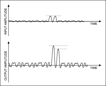
Figure 4. Memory effects.
A more common way to identify amplifier memory effects is simply to measure the output spectrum. Nonequal IM sidebands indicate amplifier memory effects (Figure 5).
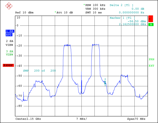
Figure 5. Amplifier output spectrum showing memory effects.
A memory-less analog predistorter can only improve the nonmemory portion of the distortion, so the amplifier has to be optimized for minimal memory effects.
There are multiple sources of memory effects and not all of them can be influenced by the circuit designer. There is not much the designer can do to minimize the heating of the LDMOS channel, but a proper cooling of the active devices which includes all drivers is helpful.
Other sources of memory effects can be mitigated by proper circuit design. A good blocking of the power supply at frequencies in the range of the modulation bandwidth is necessary to avoid changes in the supply voltage due to carrier modulation.
When optimized for maximum gain, the input-bias matching is usually optimized for high impedance but this gives the maximum influence to the nonlinear gate capacitance. If the matching is slightly detuned, amplifier gain can be lessened by some fractions of a dB. However, this can considerably reduce the memory effects. Experience² has shown that memory effects can be lowered if the amplifier is optimized for flat transfer characteristics over a much wider frequency range than the signal bandwidth. When testing the MAX2009 with commercially available PA test boards, it may be difficult to change the boards' biasing circuit. In this case it can be helpful to operate the board at a different frequency than the one for which it was optimized. Alternatively, try different frequencies within the amplifier's bandwidth. If the IM sidebands look different for different frequencies, there are memory effects caused by improper circuit design. If the amount of possible IM improvement is differen t at different frequencies, then the matching is not ideal and there is much room for further improvement.
Finally, the output impedance of the driver stage that drives into the final amplifier stage has its own influence. If a commercially available driver amplifier EV (evaluation) board is used, this board is probably optimized for high gain and efficiency if measured at a 50Ω load. The board's output impedance can differ more or less from a "real" 50Ω at the desired frequency. Thus, it is worthwhile to measure the driver's output impedance with a network analyzer and then try to minimize the output reactance by adding a shunt capacitor or inductor. In some cases this enhances the achievable amount of IM improvement for the predistorter. This is, admittedly, a rather empirical method. Nonetheless, in most cases the input impedance of the following final amplifier stage cannot be properly determined, because the required input power is too high to perform a network analyzer's measurement under real conditions.
Predistortion of Class AB Amplifiers In most current applications with nonconstant envelope modulation schemes, eg, WCDMA, Class AB amplifiers are used because they combine a much higher efficiency than Class A with a reasonable linearity.
Figures 6, 7, and 8 show an example of the output spectrum of a Class AB LDMOS PA with an LDMOS driver amplifier. The analog predistortion with the MAX2009 reduces ACPR as well as IM3.
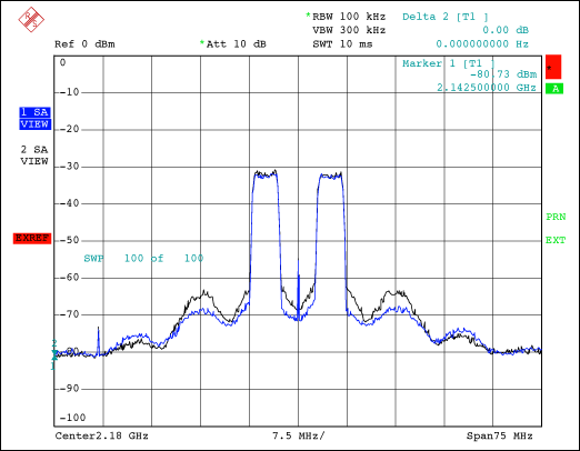
Figure 6. Output spectrum at POUT = 19W (Motorola® MW41C2230 and MRF21085).
Measurement conditions (measurement setup shown in Figure 9):
Two-carrier WCDMA signal with 3.84Mcps (3GPP)
PB_IN * = 1.46V
PF_S1 / 2 * = 4.1V
PD_CS1 * = 5V
PD_CS2 * = 0V
* See the MAX2009 / MAX2010 data sheet for an explanation of the different control voltages.
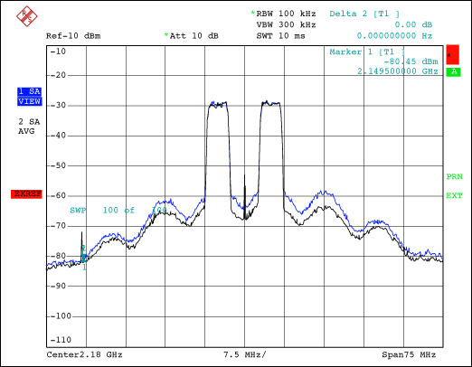
Figure 7. Output spectrum at POUT = 38W (Motorola MW41C2230 and MRF5P21180).
Measurement conditions (measurement setup shown in Figure 9):
Two-carrier WCDMA signal with 3.84Mcps (3GPP)
PB_IN = 1.52V
PF_S1 / 2 = 4.9V
PD_CS1 = 0V
PD_CS2 = 0V
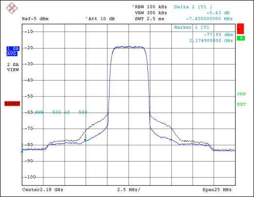
Figure 8. Output spectrum for single carrier at POUT = 19W (Motorola 21085).
Measurement conditions (measurement setup shown in Figure 9):
Single-carrier WCDMA signal with 3.84Mcps (3GPP)
PB_IN = 1.6V
PF_S1 / 2 = 5.0V
PD_CS1 = 5V
PD_CS2 = 0V
Figure 9 shows the typical measurement setup used in these experiments.
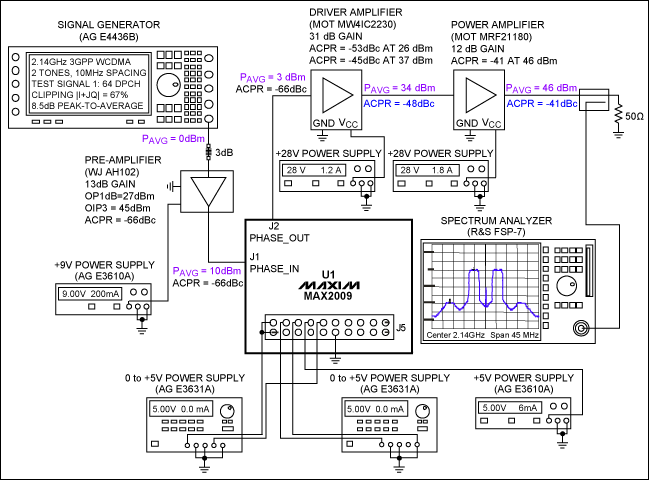
Figure 9. Typical measurement setup, Note that the ACPR values ​​do not include distortion of the MAX2009, which can be minimized by setting PB_IN to 5V.
How to Properly Adjust the MAX2009 / MAX2010The method for adjusting the MAX2009 / MAX2010 described here is not the only possible way, but it has proved to be very fast and yields optimal results.
Step 1: Insert the predistorter into your lineup. Aim for an average input power between 8dBm and 12dBm into the phase section for a 10dB peak-to-average signal. Connect the phase section only. Set PB_IN = 5V, effectively tuning the phase expansion off. Adjust the gain / attenuation after the predistorter to obtain the correct output power from your PA.
Step 2: Measure the ACPR entering the main PA. It should be at least 3dB better then the target ACPR that you are trying to achieve with predistortion.
Step 3: For a nominal slope setting (PD_CS1 = 0V; PD_CS2 = 5V; PF_S1 = 5V), slowly tune PB_IN down. Set the spectrum analyzer to a quick sweep and a low averaging (ie, averaging = 4). Lowering PB_IN raises the distortion created by the predistorter. Tune PB_IN for optimal performance. If no performance improvement is seen, then leave PB_IN at the point where performance starts to degrade.
If there is no PB_IN value for which performance degrades or improves, then the average input power into the predistorter is too low. The predistorter cannot produce distortion levels high enough. If you get ACPR degradation with PB_IN = 5V, then the average input power into the predistorter is too high.
Step 4: Fine-tune PF_S1 and PB_IN for best performance. PF_S1 biases the varactor diodes and can exceed 5V. Tune the controls to get equal IM3 / ACPR performance from both the upper and lower sideband.
If optimal performance is obtained with PF_S1> 5V, then change PD_CS2 to 0V. This should make the optimal PF_S1 voltage to be within the 5V range.
If optimal performance is obtained for PF_S1 <0.5V, then change PD_CS1 to 5V. This should make the optimal PF_S1 voltage to be greater then 0.5V. It is not desirable to have a low PF_S1 voltage because the RF signal can turn the varactor diode on. This significantly degrades performance.
Step 5: Adjust the DC bias voltage of the PA to further improve performance and efficiency. Changing the bias voltage tends to alter the lower / upper sideband power difference, as well as phase difference. This is a very important step to obtain optimal performance.
Step 6: Repeat Steps 4 and 5 until no further improvement is achieved.
The phase section exhibits some parasitic gain expansion that is dependent on the input power. This parasitic behavior can be beneficial and can provide some added improvement. Once an optimal tuning is found for the initial configuration, it may be worthwhile to experiment with different average input powers to see if a better improvement is attainable. Care must be taken, however, to make sure that a change in the average input power does not degrade the ACPR / IM3 produced by all the predrivers.
The self-heating of the amplifier alters performance. Be sure to tune the amplifier once its temperature has stabilized.
If no improvement is obtained or just to check the result of the predistortion, the compression behavior of the amplifier should be measured. This cannot be done using a network analyzer because the time between two consecutive measurement points of the gain sweep is much too long. With such a slow measurement, the amplifier has enough time to adapt to the new power level. In reality, the power level changes quickly due to the envelope of the modulation. To characterize the amplifier under real operating conditions, the distortion has to be measured using stimulus signals that show a peak-to-average ratio and a bandwidth similar to the desired modulation scheme. A software package called AMPTUNE, available from Rohde & Schwarz, ³ allows compression measurements of PAs under realistic operating conditions.
Figure 10 shows the AM-PM behavior of a 180W LDMOS transistor at an output power level of 38W before and after predistortion using the MAX2009 predistorter. In this case the application was WCDMA, so a 5MHz-wide noise signal with a peak-to- average ratio of 10dB was used as the stimulus.
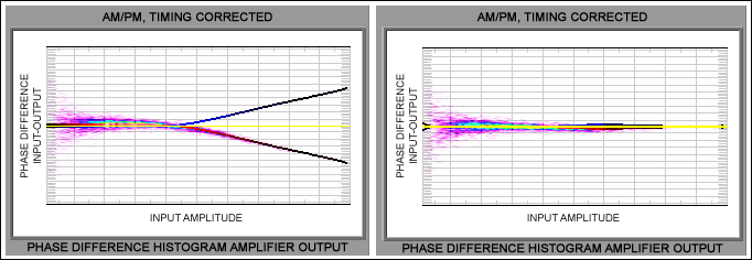
Figure 10. Phase compression measurement with AMPTUNE software.³
Please note that the software program displays the compression curve as well as the calculated expansion, which would be necessary to linearize the amplifier.
Other examples for Using the MAX2009 / MAX2010The MAX2009 / MAX2010 expands phase and gain as a function of the signal amplitude to compensate the amplifier's compression. This does not necessarily have to take place at the end frequency of a system, but can also be done in an IF stage. This approach thus expands the range of MAX2009 / MAX2010 applications from the devices' frequency range of 0.1GHz to 2.5GHz for other fields like satellite communications (Figure 11).
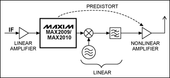
Figure 11. Predisortion with the MAX2009 / MAX2010 at the IF stage.
In Ceiling Speakers,Silk Diaphragm Tweeter,In Wall Ceiling Speakers,Two Way In Ceiling Speakers
The ASI Audio Technology Co., Ltd , https://www.asi-sound.com