![<?echo $_SERVER['SERVER_NAME'];?>](/template/twentyseventeen/skin/images/header.jpg)
Abstract: Charge pumps are often the best choice for powering an applicaTIon requiring a combinaTIon of low-power, low-voltage operaTIon and low cost. This applicaTIon note explains how to supply the MAX13041 HS-CAN transceiver with the MAX683, a 3.3V- input-to-regulated-5V-output charge pump. It also discusses the impact on electromagnetic emissions and immunity.
OverviewCompliance with the ISO 11898-2 standard for high-speed CAN communication is only guaranteed if the VCC power supply of the MAX13041 is between 4.75V and 5.25V (normal operating-voltage range). 1 That means, if CAN communication is required, a 5V rail for the CAN transceiver supply has to be available.
A familiar problem in system engineering, however, is that the subsystem's power requirements are not met by the main supply rails. In such cases, the available power rails are often not directly usable: there is only a single 3.3V supply available, or the direct use of the battery voltage is not an option for generating all required rails. Lack of space can prevent inclusion of the optimal number of supplies. In other cases, generating the 5V directly from the battery rail might not be acceptable due to heat dissipation issues , especially in systems that need CAN communication at high battery voltages (eg, during a double-battery condition in a vehicle or in a 24V truck system).
Voltage converters can generate the desired voltage levels, and charge pumps are often the best choice for applications requiring some combination of low power, simplicity, and low cost. Charge pumps are easy to use, because they do not require expensive inductors or additional semiconductors.
Selecting the Charge Pump Transceiver SuppliesThe MAX13041's VCC pin is used to supply the IC to build the proper communication signal between the bus, the voltage reference, and the receiver stage when the IC is in normal mode.
The VI / O input provides interfacing with 3.3VI / O microcontrollers to get the correct voltage level between the controller and transceiver. This pin can also be supplied by a 5V regulator, of course, when the application is communicating with such a controller.
The VBAT pin (usually connected to the car battery, 12V) supplies a very-low-quiescent wake-up detection circuit. This pin enables the MAX13041 to wake up from sleep mode on a CAN message, and it puts the transceiver in a low power mode if an undervoltage on the VBAT supply is detected.
For a detailed description of all other pins, please refer to the MAX13041 data sheet. 2
Supply CurrentsThe CAN bus can have one of two logical states: recessive or dominant (Figure 1). In normal communication mode, the MAX13041 needs a maximum VCC input current of 80mA in dominant state, and 10mA in recessive state. 3 The currents into VI / O and VBAT can get neglected.
In the presence of a bus failure, however, the VCC supply current can increase significantly, especially if the CAN_H bus line is shorted to ground. The transceiver will limit the short-circuit current to IO (SC) = 95mA.4 However, it is better to dimension the charge-pump output current for this case.
Taking the above into consideration, supplying the CAN transceiver with the proper power requires a charge pump that features an output voltage of 5V with the voltage tolerance mentioned above and a minimum output current capability of 95mA.
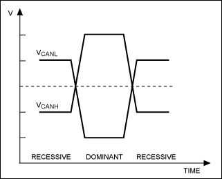
Figure 1. Logical states of the CAN bus.
3.3V-Input-to-Regulated-5V-Output Charge PumpAlthough many conventional charge-pump devices are on the market, this application note focuses on the MAX683 3.3V-input-to-regulated-5V-output charge pump to solve the power rail issue. This device delivers a regulated 5V ± 4% output voltage from an input voltage of 2.7V to 5.5V. Its switching frequency range is adjustable up to 2MHz, allowing the use of small external capacitors at 100mA output current.
The device can operate in two operating modes: skip mode and constant-frequency mode. In skip mode (the active-low SKIP input = low), switching is disabled when an output voltage higher than 5V is detected. The device then skips switching cycles until the output voltage drops. This regulation method minimizes operating current because the device does not switch continuously. In constant-frequency mode (the active-low SKIP input = high), the charge pump runs continuously at the selected frequency. This regulation scheme minimizes output ripple. Since the device switches continuously, the output noise contains well-defined frequency components, and the circuit requires much smaller external capacitors for a given output ripple. However, constant-frequency mode requires higher operating current and is less efficient at light loads than skip mode.
Example 3.3V Circuit with the MAX13041 and MAX683The circuit in Figure 2 illustrates how easy it is to supply the MAX13041 with the charge pump. The MAX683 is simply added to the VCC input of the CAN transceiver (see the dashed line), producing a 5V output voltage with the required tolerance and output current. This configuration allows the rest of the circuitry to be supplied by lower voltages. In this example, an external supply voltage of 3.3V is chosen to supply the charge pump (IN), the microcontroller, and the VI / O level translator voltage of the transceiver. The active-low SKIP input of the charge pump is pulled high, placing the part in constant-frequency mode. The switching frequency is set by the REXT resistor. The detailed dimensioning of the input / output (CIN, COUT), the flying capacitor (CX), and the frequency-set resistor (REXT) is described in the MAX683 data sheet.5
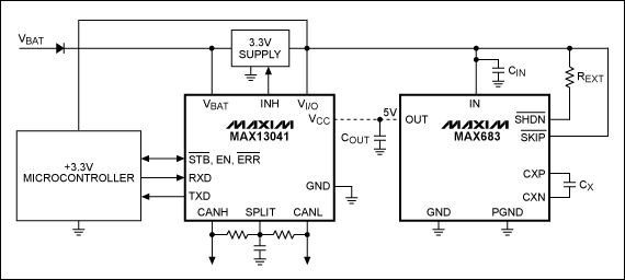
Figure 2. A circuit for supplying the MAX13041 CAN transceiver with the MAX683 charge pump.
Electromagnetic CompatibilityElectromagnetic compatibility (EMC) can be a challenge to achieve with CAN applications, especially if they are supplied with a switching voltage regulator. The wiring harness of the CAN system is particularly problematic, as the CAN_H and CAN_L pins are the interface to the bus network running into the entire vehicle. If care is not taken, one may encounter interferences, or create interferences that propagate from the CAN supply, through the transceiver, over the bus wires, and into the neighboring cables of the harness. These interferences can cause miscommunication or malfunctioning of other control units in the system.
Because of this concern, we will test the EMC behavior of the MAX13041 supplied by the MAX683 charge pump and compare it to the behavior of the standard 5V-supplied MAX13041 in order to see the impact of the charge pump in terms of EMC interferences. In this regard, we will consider two domains: electromagnetic immunity (EMI) and electromagnetic emission (EME).
Immunity TestingThe ISO 11452 specifications describe several methodologies for testing immunity to RF disturbances, including bulk current injection (BCI), transversal electromagnetic-cell (TEM-cell), stripline, and direct power injection (DPI).
We will use the DPI method because of its high reproducibility (due to the use of a well-defined test board) and the relatively low test effort needed. The principle of the DPI test is to inject a certain AC voltage into the bus lines, modulated or not, and to check the integrity of the transmitted data signal through the RXD pin of the transceiver. This method also facilitates comparison between different suppliers' designs and, moreover, is used by independent laboratories testing CAN transceivers (eg, IBEE [Ingenieur Buereo fuer industrielle Elektronik]).
Test SetupThe test setup (Figure 3) consists of three identical transceivers soldered on a defined PCB, with one of them supplied by the MAX683 charge pump. Node 1 operates as a transmitter for a bit pattern that simulates a CAN message to be received and monitored at the Rx_ output ports of all transceivers. For RF decoupling of outputs Rx1 to Rx3, as well as the input Tx1, 1kΩ resistors are used. A buffer ceramic capacitor (C = 100nF) is used at the supply ports VCC and VBAT of every transceiver IC. The resistors at the wake-up pin have a value of 33kΩ. The devices are set to normal mode by tying the pins EN and active-low STB high. The VCC voltage for node 1 is generated by the MAX683 charge-pump circuit, which is supplied with 3.3V. The 3.3V supply was also used as the VI / O voltage of transceiver node 1.
By selecting the jumper resistors R1 or R2, the charge pump can be switched between skip mode and constant-frequency mode (CFM). The switching frequency of the charge pump is set to 2MHz by the 59kΩ R3 resistor. The output capacitor C1 for the charge pump is 4.7µF, the flying capacitor C2 is 220nF, and the input IN pin is decoupled with a 470nF capacitor. In the test circuit, the bus termination is realized by a central termination using the 60Ω R4 resistor. Symmetrical RF coupling / decoupling is realized with the parallel RC combination R5 / R6 = 120Ω, C3 / C4 = 4.7nF. The external 3.3V, 5V, and 12V supplies are provided by standard power supplies, filtered by a filtering network.

Figure 3. Test setup for DPI and emissions testing.
Test ProcedureThe test is performed with the MAX13041 CAN transceivers operating in normal mode. The charge pump operates for one test run in constant-frequency mode, and in skip mode for another test run. The first test run is performed with all transceivers supplied by a standard VCC = 5V supply. A pattern generator produces a square wave with a duty cycle of 50% to simulate a CAN signal (with permanent data alternation 0-1-0) of 250kbps on the TXD pin of node 1. An HF generator on the RF input (HF1) injects an amplitude-modulated (AM) AC voltage, with a certain frequency, corresponding to a power of 36dBm into the CAN lines to simulate the disturbances.
To evaluate immunity, the RX signals of all three transceivers in the network are compared under the influence of those disturbances to the signal fed into TXD using an oscilloscope. A validation mask with a maximum allowed voltage deviation of ± 0.9V and a maximum allowed time deviation of ± 0.2µs is overlayed across the TXD signal wave shape.
If the failure criteria is true (ie, one of the transceivers' RX signals is beyond the validation mask window), the injected RF power is reduced by 0.2dBm and the same test (at the particular frequency step) is repeated until the failure criteria is false; then, the current power value is recorded and the next frequency step is adjusted. The test is carried out over a 10MHz to 100MHz frequency range. DPI Test Result Figure 4 shows the test result curves of the MAX13041 supplied by a standard 5V supply on VCC (blue), the MAX13041 supplied by the charge pump operating in constant-frequency mode (red), and the charge pump operating in skip mode (green). The X axis indicates the frequency range, while the Y axis indicates the maximum power injected without failure. As the green and the red lines are almost identical to the blue one (MAX13041 without charge pump), it can be seen that the EMI behavior of the circuit is dominated by the CAN transceiver's EMI susceptibility, rather than that o f the charge pump. Therefore, supplying the MAX13041 CAN transceiver with the MAX683 charge pump does not significantly influence the EMI behavior of the circuit.
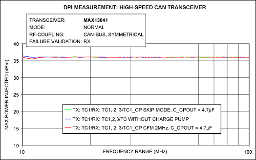
Figure 4. DPI test results.
Emissions TestingThe emissions test is performed on the same test board and test setup as the DPI test, with the exception that the power injector (HF generator) is replaced by a spectrum analyzer. The test is again performed with the CAN transceivers operating in normal mode . The charge pump is set to skip operation for one test run, and to constant-frequency mode for another one. The first test run is performed with all transceivers supplied by a standard VCC = 5V supply. The applied square wave on the CAN TXD input (simulating a transmitting bit stream of 250kbps) is maintained, and the emissions on the CAN lines are measured and recorded by the spectrum analyzer in the frequency range from 100kHz to 1GHz. The DSO is not required (Figure 3).
Emissions Test Results Figure 5 shows the resulting EME curves of the MAX13041 supplied by a standard 5V supply on VCC (blue), and supplied by the MAX683 charge pump operating in constant-frequency mode (green). Figure 6 compares the standard 5V-supplied MAX13041 (purple) with the MAX13041 supplied by the MAX683 charge pump operating in skip mode (red). The X axes indicate the frequency range, while the Y axes indicate the level of the disturbances.
As the green and the red lines (one transceiver supplied by the charge pump) again are almost identical to the lines for the MAX13041 with a standard 5V supply (blue and purple), it can be seen that the emissions behavior of the circuit is dominated by the CAN transceiver's emissions compatibility, rather than the charge pump's. These test results indicate that it is possible to supply a CAN transceiver with a charge pump without significantly influencing the overall EMC behavior of the system.
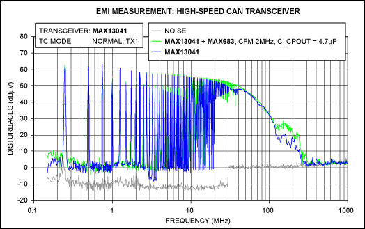
Figure 5. EME curves of the MAX13041 supplied by a standard 5V (blue), and supplied by the MAX683 charge pump operating in constant-frequency mode (green).
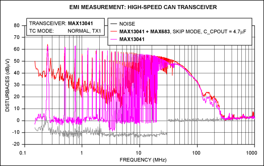
Figure 6. EME curves for the MAX13041 supplied by a standard 5V (purple), and supplied by the MAX683 charge pump operating in skip mode (red).
ConclusionIt can be challenging to achieve electromagnetic compatibility with CAN applications, especially if they are supplied by switching voltage regulators (charge pumps). However, this application note demonstrates that the EMC behavior of the circuit is governed by the CAN transceiver's EMC, rather than that of the charge pump.
Supplying the MAX13041 with the MAX683 charge pump for applications that require low-power, low-voltage operation and low cost is an option for system designers who do not have a readily available 5V power-supply rail.
References ISO 11898-2, Road vehicles—Controller area network (CAN), First Edition (2003-12-01). Data sheet for the MAX13041. Ibid. Ibid. Data sheet for the MAX683.
OverviewCompliance with the ISO 11898-2 standard for high-speed CAN communication is only guaranteed if the VCC power supply of the MAX13041 is between 4.75V and 5.25V (normal operating-voltage range). 1 That means, if CAN communication is required, a 5V rail for the CAN transceiver supply has to be available.
A familiar problem in system engineering, however, is that the subsystem's power requirements are not met by the main supply rails. In such cases, the available power rails are often not directly usable: there is only a single 3.3V supply available, or the direct use of the battery voltage is not an option for generating all required rails. Lack of space can prevent inclusion of the optimal number of supplies. In other cases, generating the 5V directly from the battery rail might not be acceptable due to heat dissipation issues , especially in systems that need CAN communication at high battery voltages (eg, during a double-battery condition in a vehicle or in a 24V truck system).
Voltage converters can generate the desired voltage levels, and charge pumps are often the best choice for applications requiring some combination of low power, simplicity, and low cost. Charge pumps are easy to use, because they do not require expensive inductors or additional semiconductors.
Selecting the Charge Pump Transceiver SuppliesThe MAX13041's VCC pin is used to supply the IC to build the proper communication signal between the bus, the voltage reference, and the receiver stage when the IC is in normal mode.
The VI / O input provides interfacing with 3.3VI / O microcontrollers to get the correct voltage level between the controller and transceiver. This pin can also be supplied by a 5V regulator, of course, when the application is communicating with such a controller.
The VBAT pin (usually connected to the car battery, 12V) supplies a very-low-quiescent wake-up detection circuit. This pin enables the MAX13041 to wake up from sleep mode on a CAN message, and it puts the transceiver in a low power mode if an undervoltage on the VBAT supply is detected.
For a detailed description of all other pins, please refer to the MAX13041 data sheet. 2
Supply CurrentsThe CAN bus can have one of two logical states: recessive or dominant (Figure 1). In normal communication mode, the MAX13041 needs a maximum VCC input current of 80mA in dominant state, and 10mA in recessive state. 3 The currents into VI / O and VBAT can get neglected.
In the presence of a bus failure, however, the VCC supply current can increase significantly, especially if the CAN_H bus line is shorted to ground. The transceiver will limit the short-circuit current to IO (SC) = 95mA.4 However, it is better to dimension the charge-pump output current for this case.
Taking the above into consideration, supplying the CAN transceiver with the proper power requires a charge pump that features an output voltage of 5V with the voltage tolerance mentioned above and a minimum output current capability of 95mA.
Figure 1. Logical states of the CAN bus.
3.3V-Input-to-Regulated-5V-Output Charge PumpAlthough many conventional charge-pump devices are on the market, this application note focuses on the MAX683 3.3V-input-to-regulated-5V-output charge pump to solve the power rail issue. This device delivers a regulated 5V ± 4% output voltage from an input voltage of 2.7V to 5.5V. Its switching frequency range is adjustable up to 2MHz, allowing the use of small external capacitors at 100mA output current.
The device can operate in two operating modes: skip mode and constant-frequency mode. In skip mode (the active-low SKIP input = low), switching is disabled when an output voltage higher than 5V is detected. The device then skips switching cycles until the output voltage drops. This regulation method minimizes operating current because the device does not switch continuously. In constant-frequency mode (the active-low SKIP input = high), the charge pump runs continuously at the selected frequency. This regulation scheme minimizes output ripple. Since the device switches continuously, the output noise contains well-defined frequency components, and the circuit requires much smaller external capacitors for a given output ripple. However, constant-frequency mode requires higher operating current and is less efficient at light loads than skip mode.
Example 3.3V Circuit with the MAX13041 and MAX683The circuit in Figure 2 illustrates how easy it is to supply the MAX13041 with the charge pump. The MAX683 is simply added to the VCC input of the CAN transceiver (see the dashed line), producing a 5V output voltage with the required tolerance and output current. This configuration allows the rest of the circuitry to be supplied by lower voltages. In this example, an external supply voltage of 3.3V is chosen to supply the charge pump (IN), the microcontroller, and the VI / O level translator voltage of the transceiver. The active-low SKIP input of the charge pump is pulled high, placing the part in constant-frequency mode. The switching frequency is set by the REXT resistor. The detailed dimensioning of the input / output (CIN, COUT), the flying capacitor (CX), and the frequency-set resistor (REXT) is described in the MAX683 data sheet.5
Figure 2. A circuit for supplying the MAX13041 CAN transceiver with the MAX683 charge pump.
Electromagnetic CompatibilityElectromagnetic compatibility (EMC) can be a challenge to achieve with CAN applications, especially if they are supplied with a switching voltage regulator. The wiring harness of the CAN system is particularly problematic, as the CAN_H and CAN_L pins are the interface to the bus network running into the entire vehicle. If care is not taken, one may encounter interferences, or create interferences that propagate from the CAN supply, through the transceiver, over the bus wires, and into the neighboring cables of the harness. These interferences can cause miscommunication or malfunctioning of other control units in the system.
Because of this concern, we will test the EMC behavior of the MAX13041 supplied by the MAX683 charge pump and compare it to the behavior of the standard 5V-supplied MAX13041 in order to see the impact of the charge pump in terms of EMC interferences. In this regard, we will consider two domains: electromagnetic immunity (EMI) and electromagnetic emission (EME).
Immunity TestingThe ISO 11452 specifications describe several methodologies for testing immunity to RF disturbances, including bulk current injection (BCI), transversal electromagnetic-cell (TEM-cell), stripline, and direct power injection (DPI).
We will use the DPI method because of its high reproducibility (due to the use of a well-defined test board) and the relatively low test effort needed. The principle of the DPI test is to inject a certain AC voltage into the bus lines, modulated or not, and to check the integrity of the transmitted data signal through the RXD pin of the transceiver. This method also facilitates comparison between different suppliers' designs and, moreover, is used by independent laboratories testing CAN transceivers (eg, IBEE [Ingenieur Buereo fuer industrielle Elektronik]).
Test SetupThe test setup (Figure 3) consists of three identical transceivers soldered on a defined PCB, with one of them supplied by the MAX683 charge pump. Node 1 operates as a transmitter for a bit pattern that simulates a CAN message to be received and monitored at the Rx_ output ports of all transceivers. For RF decoupling of outputs Rx1 to Rx3, as well as the input Tx1, 1kΩ resistors are used. A buffer ceramic capacitor (C = 100nF) is used at the supply ports VCC and VBAT of every transceiver IC. The resistors at the wake-up pin have a value of 33kΩ. The devices are set to normal mode by tying the pins EN and active-low STB high. The VCC voltage for node 1 is generated by the MAX683 charge-pump circuit, which is supplied with 3.3V. The 3.3V supply was also used as the VI / O voltage of transceiver node 1.
By selecting the jumper resistors R1 or R2, the charge pump can be switched between skip mode and constant-frequency mode (CFM). The switching frequency of the charge pump is set to 2MHz by the 59kΩ R3 resistor. The output capacitor C1 for the charge pump is 4.7µF, the flying capacitor C2 is 220nF, and the input IN pin is decoupled with a 470nF capacitor. In the test circuit, the bus termination is realized by a central termination using the 60Ω R4 resistor. Symmetrical RF coupling / decoupling is realized with the parallel RC combination R5 / R6 = 120Ω, C3 / C4 = 4.7nF. The external 3.3V, 5V, and 12V supplies are provided by standard power supplies, filtered by a filtering network.
Figure 3. Test setup for DPI and emissions testing.
Test ProcedureThe test is performed with the MAX13041 CAN transceivers operating in normal mode. The charge pump operates for one test run in constant-frequency mode, and in skip mode for another test run. The first test run is performed with all transceivers supplied by a standard VCC = 5V supply. A pattern generator produces a square wave with a duty cycle of 50% to simulate a CAN signal (with permanent data alternation 0-1-0) of 250kbps on the TXD pin of node 1. An HF generator on the RF input (HF1) injects an amplitude-modulated (AM) AC voltage, with a certain frequency, corresponding to a power of 36dBm into the CAN lines to simulate the disturbances.
To evaluate immunity, the RX signals of all three transceivers in the network are compared under the influence of those disturbances to the signal fed into TXD using an oscilloscope. A validation mask with a maximum allowed voltage deviation of ± 0.9V and a maximum allowed time deviation of ± 0.2µs is overlayed across the TXD signal wave shape.
If the failure criteria is true (ie, one of the transceivers' RX signals is beyond the validation mask window), the injected RF power is reduced by 0.2dBm and the same test (at the particular frequency step) is repeated until the failure criteria is false; then, the current power value is recorded and the next frequency step is adjusted. The test is carried out over a 10MHz to 100MHz frequency range. DPI Test Result Figure 4 shows the test result curves of the MAX13041 supplied by a standard 5V supply on VCC (blue), the MAX13041 supplied by the charge pump operating in constant-frequency mode (red), and the charge pump operating in skip mode (green). The X axis indicates the frequency range, while the Y axis indicates the maximum power injected without failure. As the green and the red lines are almost identical to the blue one (MAX13041 without charge pump), it can be seen that the EMI behavior of the circuit is dominated by the CAN transceiver's EMI susceptibility, rather than that o f the charge pump. Therefore, supplying the MAX13041 CAN transceiver with the MAX683 charge pump does not significantly influence the EMI behavior of the circuit.
Figure 4. DPI test results.
Emissions TestingThe emissions test is performed on the same test board and test setup as the DPI test, with the exception that the power injector (HF generator) is replaced by a spectrum analyzer. The test is again performed with the CAN transceivers operating in normal mode . The charge pump is set to skip operation for one test run, and to constant-frequency mode for another one. The first test run is performed with all transceivers supplied by a standard VCC = 5V supply. The applied square wave on the CAN TXD input (simulating a transmitting bit stream of 250kbps) is maintained, and the emissions on the CAN lines are measured and recorded by the spectrum analyzer in the frequency range from 100kHz to 1GHz. The DSO is not required (Figure 3).
Emissions Test Results Figure 5 shows the resulting EME curves of the MAX13041 supplied by a standard 5V supply on VCC (blue), and supplied by the MAX683 charge pump operating in constant-frequency mode (green). Figure 6 compares the standard 5V-supplied MAX13041 (purple) with the MAX13041 supplied by the MAX683 charge pump operating in skip mode (red). The X axes indicate the frequency range, while the Y axes indicate the level of the disturbances.
As the green and the red lines (one transceiver supplied by the charge pump) again are almost identical to the lines for the MAX13041 with a standard 5V supply (blue and purple), it can be seen that the emissions behavior of the circuit is dominated by the CAN transceiver's emissions compatibility, rather than the charge pump's. These test results indicate that it is possible to supply a CAN transceiver with a charge pump without significantly influencing the overall EMC behavior of the system.
Figure 5. EME curves of the MAX13041 supplied by a standard 5V (blue), and supplied by the MAX683 charge pump operating in constant-frequency mode (green).
Figure 6. EME curves for the MAX13041 supplied by a standard 5V (purple), and supplied by the MAX683 charge pump operating in skip mode (red).
ConclusionIt can be challenging to achieve electromagnetic compatibility with CAN applications, especially if they are supplied by switching voltage regulators (charge pumps). However, this application note demonstrates that the EMC behavior of the circuit is governed by the CAN transceiver's EMC, rather than that of the charge pump.
Supplying the MAX13041 with the MAX683 charge pump for applications that require low-power, low-voltage operation and low cost is an option for system designers who do not have a readily available 5V power-supply rail.
References ISO 11898-2, Road vehicles—Controller area network (CAN), First Edition (2003-12-01). Data sheet for the MAX13041. Ibid. Ibid. Data sheet for the MAX683.
The iPhone series battery stickers are used to avoid the battery from static electricity, guard your cell phone and helpful to easy removal of battery.
IPhone 5/5S/SE/6/6S/7 Battery Glue Adhesive
IPhone Battery Glue Adhesive,Battery Glue Adhesive,IPhone Tape Stripe
Shenzhen Aokal Technology Co., Ltd. , https://www.aokal.com