![<?echo $_SERVER['SERVER_NAME'];?>](/template/twentyseventeen/skin/images/header.jpg)
IntroductionThis application note applies to the following products:
| T1 Framers | T1 SCTs |
| DS2141A | DS2151 |
| DS21Q41B | DS2152 |
| DS21Q42 | DS21352 |
| DS21FF42 | DS21552 |
| DS21FT42 | DS21Q352 |
| DS21Q352 |
All Dallas Semiconductor T1 framers and single-chip transceivers (SCTs) provide support for D4 framing and signaling, as shown in Figure 1. This application note provides the requirements to enable the D4 format in the transmit and receive paths for T1 framers and SCTs.
For the transmit path, programming the registers for framing and signaling operations are discussed. For the receive path, programming the registers to retrieve framing and signaling is discussed along with receive interrupt handling.
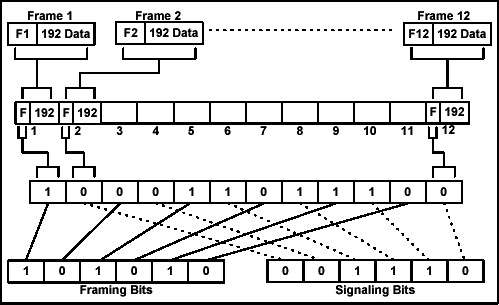
Figure 1. D4 framing format. D4 Framing Register SettingsSeveral registers must be initialized to enable D4 multiframing. Table 1 shows the register settings required to generate and receive D4 multiframing.
Table 1. D4 Framing Register Settings
| Register Setting | Function |
| CCR2.7, CCR2.3 = 0 | Selects D4 multiframing in the transmit and receive directions. |
| CCR2.5 = 1 | Enables insertion of the 6-bit Fs pattern. |
| TFDL = 1Ch | This is the 6-bit Fs pattern. |
| RCR1.3 = 1 | If this bit is cleared, the receiver declares synchronization on the Ft pattern only and will not be guaranteed to find the D4 multiframe boundary. |
| Toggle low to high RCR1.0 | Required after configuring the control registers to force resynchronization. |
Table 2. Transmit Signaling Registers
| Register | Description |
| TS1 and TS7 | A bits for channels 1 through 8 |
| TS2 and TS8 | A bits for channels 9 through 16 |
| TS3 and TS9 | A bits for channels 17 through 24 |
| TS4 and TS10 | B bits for channels 1 through 8 |
| TS5 and TS11 | B bits for channels 9 through 16 |
| TS6 and TS12 | B bits for channels 17 through 24 |
Table 3. Transmit Signaling Register Map (D4 Format)
| (MSB) | (LSB) | |||||||
| TS1 (70h) | CH8-A | CH7-A | CH6-A | CH5-A | CH4-A | CH3-A | CH2-A | CH1-A |
| TS2 (71h) | CH16-A | CH15-A | CH14-A | CH13-A | CH12-A | CH11-A | CH10-A | CH9-A |
| TS3 (72h) | CH24-A | CH23-A | CH22-A | CH21-A | CH20-A | CH19-A | CH18-A | CH17-A |
| TS4 (73h) | CH8-B | CH7-B | CH6-B | CH5-B | CH4-B | CH3-B | CH2-B | CH1-B |
| TS5 (74h) | CH16-B | CH15-B | CH14-B | CH13-B | CH12-B | CH11-B | CH10-B | CH9-B |
| TS6 (75h) | CH24-B | CH23-B | CH22-B | CH21-B | CH20-B | CH19-B | CH18-B | CH17-B |
| TS7 (76h) | CH8-A | CH7-A | CH6-A | CH5-A | CH4-A | CH3-A | CH2-A | CH1-A |
| TS8 (77h) | CH16-A | CH15-A | CH14-A | CH13-A | CH12-A | CH11-A | CH10-A | CH9-A |
| TS9 (78h) | CH24-A | CH23-A | CH22-A | CH21-A | CH20-A | CH19-A | CH18-A | CH17-A |
| TS10 (79h) | CH8-B | CH7-B | CH6-B | CH5-B | CH4-B | CH3-B | CH2-B | CH1-B |
| TS11 (7Ah) | CH16-B | CH15-B | CH14-B | CH13-B | CH12-B | CH11-B | CH10-B | CH9-B |
| TS12 (7Bh) | CH24-B | CH23-B | CH22-B | CH21-B | CH20-B | CH19-B | CH18-B | CH17-B |
Table 4. Receive Signaling Registers (D4 Format)
| (MSB) | (LSB) | |||||||
| RS1 (60h) | CH8-A | CH7-A | CH6-A | CH5-A | CH4-A | CH3-A | CH2-A | CH1-A |
| RS2 (61h) | CH16-A | CH15-A | CH14-A | CH13-A | CH12-A | CH11-A | CH10-A | CH9-A |
| RS3 (62h) | CH24-A | CH23-A | CH22-A | CH21-A | CH20-A | CH19-A | CH18-A | CH17-A |
| RS4 (63h) | CH8-B | CH7-B | CH6-B | CH5-B | CH4-B | CH3-B | CH2-B | CH1-B |
| RS5 (64h) | CH16-B | CH15-B | CH14-B | CH13-B | CH12-B | CH11-B | CH10-B | CH9-B |
| RS6 (65h) | CH24-B | CH23-B | CH22-B | CH21-B | CH20-B | CH19-B | CH18-B | CH17-B |
| RS7 (66h) | CH8-A | CH7-A | CH6-A | CH5-A | CH4-A | CH3-A | CH2-A | CH1-A |
| RS8 (67h) | CH16-A | CH15-A | CH14-A | CH13-A | CH12-A | CH11-A | CH10-A | CH9-A |
| RS9 (68h) | CH24-A | CH23-A | CH22-A | CH21-A | CH20-A | CH19-A | CH18-A | CH17-A |
| RS10 (69h) | CH8-B | CH7-B | CH6-B | CH5-B | CH4-B | CH3-B | CH2-B | CH1-B |
| RS11 (6Ah) | CH16-B | CH15-B | CH14-B | CH13-B | CH12-B | CH11-B | CH10-B | CH9-B |
| RS12 (6Bh) | CH24-B | CH23-B | CH22-B | CH21-B | CH20-B | CH19-B | CH18-B | CH17-B |
Receive Multiframe Interrupt (RMF): The RMF bit in Status Register 2 (SR2.7) is set and the bits in the receive signaling registers are updated on receive multiframe boundaries. Therefore, the RMF interrupt can be used to determine when to retrieve the receive signaling registers. Setting bit 7 of the Interrupt Mask Register 2 (IMR2.7) enables the RMF interrupt. Receive Signaling Change Interrupt (RSC): The RSC bit in Status Register 2 (SR2.0) is set when a change of sate is detected in any of the signaling bits. Setting bit 0 of the Interrupt Mask Register 2 (IMR2.0) enables the RSC interrupt. Once a signaling change has been detected, the user has at least 2.75ms to read the data before it is lost. When responding to an RMF or RSC interrupt, the most recent multiframe of signaling is available in RS7 through RS12, not RS1 through RS6. The receive signaling registers are frozen and not updated during a loss-of-sync condition (SR1.0 = 1). They contain the most recent signaling informat ion before the "OOF" occurred. The signaling data reported in RS1 to RS12 is also available at the RSIG and RSER pins. D4 Framing and Signaling Information For more information about Dallas Semiconductor's T1 framers and SCTs, please consult the data sheets available on our website at
If you have further questions concerning the operation of our T1 framers or SCTs, please contact the Telecommunication Applications support team via email at var name = "telecom.support @"; var domain = "dalsemi.com"; document.write ("" + name + domain + ""); telecom. or call 972-371-6555.
Disposable Medical Masks
FDA&CE certificate
Suitable for respiratory protection, filtering dust, haze, bacteria, droplets and other harmful particles in the air.


HIGH QUALITY – The filter membrane is made of safety standard materials, three-layer disposable masks, which can be used by children and adults, can maintain health and safety when working or going out, can well protect the health of the respiratory system and protect your breathing.
FAQ:
Advantages:
1. WE ARE FACTORY! We have our ownshare factory in shenzhen, Very welcome to visit if available.
2. OEM & ODM
3. Short delivery time
4. Environmentally-friendly material
5. Good workmanship
6. We always ship by international express, air and sea.
7. We serve with best quality and service.
Shenzhen Dianjiang Engineering Co. LTD , https://www.isourceled.com