![<?echo $_SERVER['SERVER_NAME'];?>](/template/twentyseventeen/skin/images/header.jpg)
Two inductors are often used in mobile power supplies on the market. In the charging circuit, the charging process requires an inductor, and the Boost circuit also needs an inductor during discharge. The working process of the charging circuit is to charge the lithium battery inside the mobile power source through the 5V AC adapter; and the Boost circuit works by boosting the internal lithium battery of the mobile power source to 5V for output, thereby supplying power to the mobile device. However, in the actual operation of the mobile power supply, the two circuits usually do not need to work at the same time, that is, only one inductor of the two inductors is in operation, and only one operation is needed for the two loops.
1. How the chip works
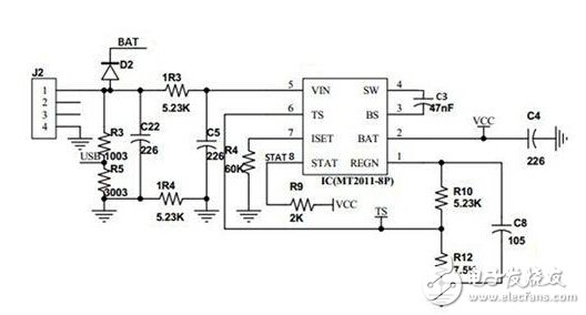
This paper proposes a single-inductor mobile power supply solution, which not only helps the mobile power source to save device cost, but also saves equipment size and facilitates the miniaturization of the mobile power supply. To make the equipment more stable, the single-inductor mobile power circuit is shown in Figure 1:
(a) Charging chip peripheral circuit

(b) boost chip peripheral circuit

(c) MCU peripheral circuit
Figure 1. Chip working circuit in the circuit
MT2011 is a high efficiency and high current single series lithium battery charge controller designed by Laiyu Technology. It supports 4.5V~6.5V input voltage, the output voltage can follow the lithium battery voltage, the maximum 2A charging current, using a high efficiency synchronous rectification structure, suitable for portable charging equipment and mobile power charging. Integrate current sampling resistors, high-precision current and voltage management circuits, and fully stop charging at full power. MT2011 operating frequency is 1.5MHz, using synchronous rectification structure, the efficiency is up to 93%. With charging current soft start, anti-inverting current diode, charging current sampling and other functions, with complete output short circuit protection and over temperature protection.
The MT5036 is a 95% efficient 800KHz synchronous boost converter designed by Lai Technology, which provides a good power supply solution for parallel connection of single-cell lithium batteries or multi-cell lithium battery packs. The converter obtains a stable output voltage by setting the chip's external FB divider resistor or by using an internal FB divider resistor. The chip conversion efficiency is very high, can provide enough load current, when the supply voltage drops to 3V, it can still output 3A load current when the output voltage is 5V, the peak current in the inductor is limited to 6.6A.MT5036 working frequency Up to 800KHz, which makes the inductor and output capacitors not too large, and with light load PSM function, can ensure the chip to maintain high conversion efficiency in the full load range. With 60uA quiescent current, it can greatly improve the life of lithium battery, with low EMI working mode, can effectively reduce ringing when working intermittently, converter can avoid over-discharge of battery, load can be completely disconnected from battery when shutting down open.
SN8P2711 is an 8-bit high-performance simplification instruction microcontroller designed and developed in high-speed low-power CMOS process. It has 1K&TImes; 16-bit one-time programming ROM (OTP-ROM), 64K & TImes; 8-bit data register (RAM), three Two bidirectional I/O ports, two 8-bit timer/counters, two PWM/Buzzer modules, multiple system clocks, four system operating modes, one five-channel twelve-bit analog-to-digital converter, and five interrupt sources . This MCU can be widely used in measurement, motor control, industrial control, home appliances and toys.
3. Analysis of circuit working principle
The specific working principle of the circuit is as follows:
The circuit work is divided into two processes. One is to add a 5V power supply to charge the built-in lithium battery of the mobile power source, and the other is to charge the mobile power to the external mobile device.
When working in the first process, the AC adapter or 5V power supply is connected to the Micro USB interface of the mobile power supply. When VIN is 5V, the R1 and R2 voltage dividers generate a USB signal and send it to the MCU. After the MCU detects the USB signal, it will The output EN signal is pulled low, prohibiting the MT5036 from operating. MT2011 will detect the voltage of VCC after power-on. If the VCC voltage is within the chargeable range, the charging chip will start to work. The lithium battery will start charging according to the process of floating charge, fast charge and constant voltage charge, and the inductor current will be charged from SW to VCC. The TS signal is high by default. If the external circuit causes TS to be pulled low to let MT2011 stop working, D2 is a clamp diode that can limit the SW voltage to at least -0.6V. Figure 2 shows the charging and discharging process signals and input and output. Timing diagram.
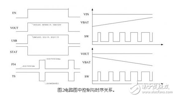
When working in the second process, no AC adapter is connected to the USB 2.0 port to connect the charged device. That is, the VOUT of the MT5036 is only connected to the device being charged. The circuit will detect if the portable device is connected to the USB2.0 port. If the device is plugged in or press the start button, the MT5036 will be activated to charge the device. VCC in the circuit is connected to VOUT through R24 (100K).
When the mobile power output port is not connected to the device, the VOUT voltage is equal to the VCC voltage. At this time, the EN signal of the MT5036 is low, and the chip does not work. When the device is plugged in, VOUT is pulled low by the device instantaneously. When the MCU detects that VOUT is low, it can be judged that the device has been connected, and the EN signal is pulled high to enable MT5036 to work and charge the device. When EN goes high, the STAT signal is forced to pull low. At this time, MT2011 can be disabled to ensure that the charge and discharge chip can work at most.
When the MT5036 is working, the inductor current is pulled down from VCC to SW.R9 to ensure that the EN pin can be grounded when the EN is left floating for some reason. The MT5036 will not malfunction. R7 and R8 are the voltage divider resistors of FB, and the VOUT voltage of MT5036 is set by these two resistors. C9, C10, C11 are output storage capacitors, BOOST circuit inductors are not continuous to the output terminal, and the output capacitor capacity should be selected as large as possible. Two 22uF chip capacitors are used in parallel in the MT5036 chip. R14, R15 are output current sampling resistors, which can sample the load of MT5036 to judge the overload or no-load condition.
When the AMP signal voltage exceeds the overload threshold, the MCU judges that it is overloaded. At this time, EN is pulled low and the off section is MT5036. When the AMP signal voltage is lower than the 0.1A load threshold, the MCU judges to be no-load, to prevent efficiency dissipation, 40s After the EN is also pulled low, off section MT5036.
The relationship between the output voltage and the voltage divider resistor is:

When the mobile power supply is working in the charging process, SW is the square wave signal of VIN and GND, and the VBAT pin is the internal power supply pin of MT5036. If the VBAT pin is the battery voltage, there will be internal leakage current, which may occur. Caused damage to the MT5036. As can be seen from Figure 1(a), the power adapter 5V input (VIN) and the lithium battery output (VCC) are both diode-connected to the MT5036's VBAT pin. This can prevent leakage inside the chip. After adding these two diodes, the power supply pin of MT5036 will select the side with the larger voltage as the power supply, which can ensure the effective closing of the internal MOS tube. The type of diode is preferably a Schottky diode.
The MCU functions to adjust the working mode and protection in the mobile power supply. The SW1 of the 7th pin of the MCU is the switch of the mobile power output. When the switch is pressed, the EN signal is pulled high to make the MT5036 work. Four LED lights are used to display the current power and charge and discharge status of the mobile power. The SW1 switch can also be turned on by a long press of the mobile power flashlight.
4. Experimental results and analysis
This paper proposes a single-inductance high-efficiency mobile power supply design that has been widely used in mobile power supplies on the market. The use of 1 ounce copper thick double-layer PCB indicators has been able to meet the requirements.
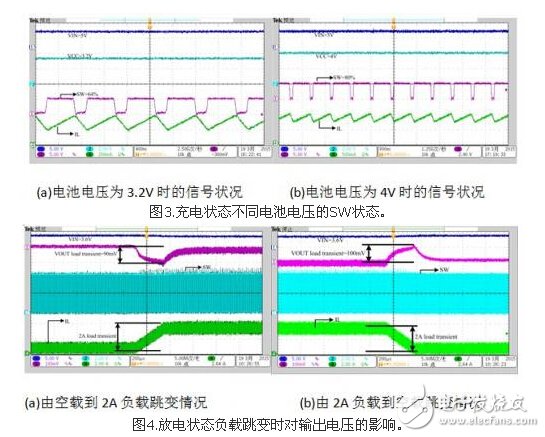
The variable duty cycle with battery voltage keeps the system stable in the input and output range, as shown in Figure 3. SW duty cycle can be maintained at D = VOUT / VIN. The entire system is stable
As can be seen from Figure 4, the load jump of 2A will cause an output change of less than 100mV, which is a 2% rate of change, which is very good in mobile power chips.
In the charging process, the highest efficiency can reach 92%; in the discharge process, the highest efficiency can reach 96%. Therefore, using MT2011 and MT5036 two power chips can make the overall equipment maintain high efficiency. When the chip is in standby state, the quiescent current can be as low as 40uA, which means that it is in standby state for 180,000 hours, which consumes 25% of the power of the mobile power, so the system can maintain a long life.
5 Conclusion
In this article, through the introduction of the two power chips of Lai Technology and the introduction of the overall circuit working state, a mobile power supply design scheme for charging and boosting single inductor applications with low quiescent current is described.
The system can keep the mobile power system stable in a single inductor (low cost). And can maintain up to 96% discharge efficiency. The low quiescent current of 40uA allows the mobile power supply to have an extremely long life. The single-inductor mobile power supply described in this article also has a self-starting function for the plug-in appliance, and the 2A load jump (ipad insertion or removal) can maintain the 2% output accuracy.
Description of bouncing doll cover sleeve
This kind of jumping boucing doll can make the kids so strange because of its jumping by itself.
1. Round Pet Braided Expandable Sleeve
2. Green and Halogen Free
3. Flexible and Lightweight
4. Cut with Different Length According to Client's Requirements
5. Popular to Kids Playing
Boucing doll sleeve's material is PET Expandable Braided Sleeve compiled by the Environmental Protection PET filament diameter monofilament 0.20mm or 0.25mm's made with good flexibility, flame resistance, abrasion resistance and heat resistance, network management can be easily expanded to the original 150% , and it is easy to tighten the various irregularly shaped objects, which can be maintained within a wide temperature range while maintaining a soft, can inhibit chemical corrosion, UV and friction, characterized by its unique mesh also has good ventilation, wire heat diffusion function in a timely manner.
Jump Doll Sleeve,Jump Doll Sleeving,Jump Kid Toy ,Sleeve For Bouncing Doll
Shenzhen Huiyunhai Tech.Co.,Ltd , https://www.hyhbraidedsleeve.com